![[TOC]](PIC/toc.gif)
This is my Master of Science Thesis for the Electronics and Telecommunications Engineering Department of the Electrical and Electronics Engineering Faculty of the Istanbul Technical University, Istanbul, Turkey. This version is slightly different from the original thesis, it has a nicer layout, and a modified preface. I am also working on an online version of this thesis which will hopefully be available at the URL:
http://turquoise.wpi.edu/aries
I would like to thank especially to Yusuf Leblebici, who has been my much travelling advisor. The Heisenberg Principle of Uncertainity definitely applies to him: If you know where he is, you don't know what he is doing, and if you know what he is doing you don't know where he is.
A big special thank you to my family, who have always been with me and supported me and to Öden Hotin who has treated me like his own child and protected me in Switzerland.
I would also like to thank my professors at the ITU (in no particular order): Erdal Panayýrcý, for helping me with my average :-); Duran Leblebici, it is called HAL - not HALL; Uđur Çilingirođlu, for talking me into staying at ITU; Osman Palamutçuođullarý, for keeping me interested in electronics; Bülent Örencik, for being an extremely nice person; Ergül Akçakaya, for the trust he put in me; Hakan Özdemir, you still owe me 10 Guiness.
I also want to mention my co-workers at the ITU: Bilgin, is that an Amiga ?; MVT, what do you mean by saying I can complete the missing parts ?; Bülent, I can't be ugly; Asým, Nafý yani?; Elif, This is Çomar, my cat; Murat, I need someone who understands from computers, to help me carry this PC; Ece, Let us go to the mining faculty for breakfast; Cem, the speedy sports reporter; Selçuk, Dear admin I have a question; Hakan, let us drink and be beautiful, Barýţ, Foton at your service, Bilge, do you call that a layout, and Müţtak, from 10am Sunday to 1am Thursday, is that the faculty record ?
I'd like to thank to Daniel Mlynek, for accepting me as a refugee and providing a splendid working environment, all the friends at C3i-DE-EPFL: Alex, Alain, Paul, Theo, Francesco, Christophe, Laurent, Seong, Marc, Martin, Sophie, Frederic, Stephanie, Sylvain and Giorgio.
And last but not least to all my friends, for making my life so special: Erhan, Özlem, Orhan, Nezaket, Esra, Harun, Tandođan, Turgut, Ţima, Tuna, Nil, Berna, Torrence and the Dutch Gang, the Turkish Linux Users Group and all the rest that I forgot to mention.
Thank You !
January 1998
Frank Kagan Gürkaynak
Digital Signal Processing has evolved into one of the main applications of current VLSI technology. The recent developments within the electronics industry has resulted in new applications which require extensive signal processing. These applications have entered the consumer market that has placed a high demand especially on multimedia applications.
Most of the digital signal processing operations can be expressed by means of convolutions where the image data value and a set of neighbouring data values are convolved by a set of coefficients. This operation is especially computation intensive as it involves a number of multiplications. For high bandwidth signals such as images, these operations have to performed repedeatly over a large set data continously. As a result, the general nature of this operation requires a number of area consuming high speed multipliers.
In this work, a basic building block for the construction of convolutional filtering blocks is presented. This block (named Aries) uses pre-calculated values stored in a RAM to compute the result of a 5x1 kernel. These blocks can be combined to generate a filter of any dimensions 1-D or 2-D). Aries includes an output stage that can be used to generate a pipelined adder array to sum up the results of all Aries blocks. The block operates on 8-bit unsigned data at a rate of 50 million samples per second. This corresponds to an equivalent performance of 450 MOPS (Million Operations per second). A 9x9 filter realization would only need 18 Aries blocks, have an equivalent performance of more than 8 GOPS (Giga Operations Per Second) and occupy a silicon core area of less than 30 mm^2 even in a modest 0.8um CMOS technology. The Full-Custom design methodology employed throughout the design is presented as well.
Digital Signal Processing (DSP) technology is one of the more recent developments of the fast evolving electronics technology and yet it is increasingly used in daily life. Celullar telephones, modems, CD-ROM devices, audio equipment, hard disks and automobile electronics are examples of the broad spectrum of the broad application spectrum of DSP devices [1]. The first programmable DSP processors appeared in the early 80's and were intended as audio processors. Within ten years the processing power of custom digitial signal processing hardware has became capable of processing video rate signals. The development of multimedia applications and standarts led to another development where recently general purpose processors started including specialized hardware to acquire basic signal processing capability.
Even the most simple DSP algorithms require extensive computation and DSP operations in general are still considered to be among the most demanding operations in integrated circuit technology. A typical DSP operation consists of a series of multiplications on stored values of input data with a set of co-efficients, producing results which are then accumulated. As the signal has to be processed continously, the bandwidth of the signal puts strict constraints on the speed of operation. As an example, for video applications 10 to 75 pictures need to be processed each second. Depending on the resolution each picture may have as many as two million pixels, where each pixel is represented by (at least) 8 bits. Any video processing algorithm will therefore need to calculate the result of the operation on the order of tens of nanoseconds.
High performance digital signal processing architectures rely on complicated designs, that are usually tailored for a particular application. Moreover, these designs are rather large and have transistor counts on the order of millions of transistors. These designs are usually parts of a custom chip-set for a specific application such as MPEG decoding. It is extremely hard to adapt these designs for new requirements as most of them have application oriented optimizations.
In this work, a programmable, fully pipelined compact LSI macro block (Aries) is presented, that can be used to design 1-D or 2-D convolutional filters of any size with a clock cycle of 20 ns. The design is extremely compact and occupies an active silicon area of less than 1.5mm^2 in a conventional 0.8um digital CMOS technology. Several Aries macro-blocks can therefore easily be embedded in a larger design. The fully pipelined 20 ns-cycle operation time is sufficient for high resolution image processing. Aries is fully programmable (at a lower speed than the data input rate), which gives it an adaptive filtering capability. Aries also includes the hardware necessary to accumulate the results of several Aries chips and can easily be scaled to accommodate digital filters of any dimensions.
There are three basic alternatives for the construction of digital filters [2]. The commonly used two alternatives employ multipliers. In Aries there are no multipliers, the data is broken down into its bitplanes. The data-bits of the same order are grouped to form a RAM address, and a pre-computed partial result is read from a RAM. The partial results corresponding to these data-bits are then weighted and accumulated in an adder array to form a result.
In Chapter 2, a brief introduction to Digital Signal Processing is given,with an emphasis on the binary number systems used in digital systems. Aries is developed from earlier work on Taurus, A Capacitive Threshold Logic based image filter [3]. Chapter 3 shortly describes the basic architecture of Taurus and discusses the main problems encountered during design. The design of Aries is explained in detail in Chapters 4 (general structure), Chapter 5 (RAM design), Chapter 6 (adder design) and Chapter 7 (Implementation). As a speed and area optimized design, Aries has been designed using a full-custom design methodology. Some aspects of this design methodology are explained using the design of one of the main blocks of Aries in Chapter 8. Finally, Chapter 9 summarizes all the results.
Throughout the entire science history man has tried to understand, analyze, imitate and most of all, control its surrounding environment. The limits of human capabilities were the dominant factorsfor most of the technical inventions. They felt cold, understood that fire would provide the necessary heat and then they went on to generate fire and control it. There are many key inventions that has had a key role in the history of civilization: the wheel, the invention of writing, bronze, gunpowder, the steam engine and integrated circuits have all changed the way of life dramatically. Today, thanks to the extended usage of integrated circuits, we are said to be living in an information age.
A very important breakthrough in information processing came with the introduction of integrated digital circuits. Digital circuits, unlike their analog counterparts, interpret their inputs as one of two logic states: logic "1" and logic "0". The output of any digital circuit comprises of a set of these states. These two states are enough to define a binary number system where any mathematical operation can be realized, which makes digital circuits ideal candidates for computational operations. Furthermore digital information is much more noise immune than analog signals and there are practically lossless methods to store digital states. There is only one slight problem:
Every piece of natural information is strictly analog in nature: they consist of continuous signals. Fortunately it is quite easy to express any analog value in terms of a number of digital states. Analog to Digital Converter (ADC) circuits are used to make this conversion. The digital circuits can then process, store and manipulate these analog signals. Once a result is available Digital to Analog Converter (DAC) circuits can convert the digital value into an analog signal.
Digital Signal Processing, is a general term that describes specialized algorithms for signal processing using digital circuits. These signals can range from low frequency audio signals to high resolution image image signals. Most DSP applications can be described as various filtering algorithms to enhance the original signal. Applications include:
Especially new multimedia applications and standarts (eg. MPEG2, MPEG4) require computation-intensive transformations to reduce the bandwidth and to enhance the quality of audio and video signals.
The basic digital unit is called a bit. One bit can only have one of the two values: logic "0" or logic "1" (commonly referred to as 0 and 1). It is evident that one bit alone can not hold much information. More bits can be joined to form a number that can express larger numbers. With a total of n bits 2^n different numbers can be expressed. Yet this alone does not describe how a number can be represented in digital form. There are several number systems with different capabilities and short-comings
The binary number systems are the most widely used number systems because of their simplicity. The basic binary number system is much similar to the decimal system we use. An n-bit number in the binary number system is an ordered sequence of bits:
 (2.1)
(2.1)
This number exactly represents an integer or fixed-point number. If we consider only natural numbers, a direct representation would be possible. This is called an unsigned binary number representation. For a set of a(i) the corresponding value can be calculated as:
 (2.2)
(2.2)
Numbers from 0 to 2^n-1 can easily be represented this way. If negative numbers are involved, a different approach needs to be taken. A solution analogous to the solution used in a decimal number system would be to use a digit to represent the sign. This representation, where the Most Significant Bit (MSB) of the sequence represents the sign of the number, is called the Sign-Magnitude Binary Number system. The value of A can be determined by:
 (2.3)
(2.3)
Although this format is relatively easy to comprehend, it has some important disadvantages. The number 0 can be represented in two different ways (one with a positive and one with a negative sign). A more significant problem is that positive numbers and negative numbers have to be treated differently in arithmetic operations. This is a major problem for operations that involve more than two operands, as the number of possibilities for the signs increase dramatically with the increasing number of operands.
The Two's Complement representation of the binary number system is the more frequently preferred alternative to represent both positive and negative numbers. The value of A of a two's complement number can be calculated by the following method:
 (2.4)
(2.4)
The negative value of any number with this representation can be calculated as:
 (2.5)
(2.5)
The most interesting feature of this representation is that for most of the basic arithmetic operations, digital computation blocks (with slight limitations) will perform correctly independent of the sign of the number. Table 2.1 gives all the combinations of a 4-bit number and lists their respective values for the three representations.
Table 2.1:Values of a 4-bit number according to its representation.
Bit sequence    Unsigned     Sign-Magnitude  Two's Complement
    0000            0            +0                0
    0001            1             1                1
    0010            2             2                2
    0011            3             3                3
    0100            4             4                4
    0101            5             5                5
    0110            6             6                6
    0111            7             7                7
    1000            8            -0               -8
    1001            9            -1               -7
    1010           10            -2               -6
    1011           11            -3               -5
    1100           12            -4               -4
    1101           13            -5               -3
    1110           14            -6               -2
    1111           15            -7               -1
The most important disadvantage of the binary number representation is that for some small change in value, a large number of bits within the number may change. As an example for a 8 bit number, consider the representation of 63 (0011 1111) and 64 (0100 0000) (notice that this example is independent of the number representation). Although the distance between these two numbers is only one LSB, 7 out of 8 digits have changed their values.
The Gray number system is a non-monotonic representation where two consecutive numbers differ in only one of their digits. For some applications such as counters or low-power address bus decoders the Gray number system can help reduce the power consumption as for consecutive numbers there will be fewer transitions (and associated power consumption).
The main disadvantage of this number representation is that it is not well suited for arithmetic operations mainly because Gray numbers are non-monotonic. The lower power consumption issue is also arguable, as the extra power used for the generation of Gray numbers may decrease the aforementioned power savings considerably [4].
Addition is by far the most important elementary operation with in digital systems. The main difficulty with the addition lies in the carry problem (also referred as the curse of carry) [1]. The result of an operation on the bits of same magnitude can affects the result of higher order bits and is likewise affected by the result of lower order bits.
The redundant number systems are a result of this problem. The main idea is to represent one digit with more than one bits (hence the name redundant) to avoid carry propagation in adders. As a result of redundant bits, a number represented in a redundant number system has higher storage requirements than that of a number represented in a non-redundant form. A second disadvantage is that the conversion from a redundant number system to non-redundant number system is quite complicated.
All the number systems discussed so far are so-called fixed point number systems. The floating point representation consists of a sign bit (S), a mantissa (M) and an exponent (E) in the form of:
 (2.6)
(2.6)
Table 2.2 shows two IEEE standarts for floating point representations.
Table 2.2 IEEE Floating point standart.
Standart    n    M bits    E bits   Range    Precision

single      32     23        8      3.8E+38     1E-7
double      64     52       11      9.0E+307    1E-15
Floating point operations require different operations for mantissa and exponent parts of the number. General purpose processors which are used for scientific computing make use of floating point arithmetics by means of dedicated Floating Point Units (FPU) to speed up computation intensive applications. Not more than five years ago these FPU's were usually auxiliary processors. Today all of the modern general purpose processors have embedded FPU blocks.
There are other number representations such as: Residue Number System, Logarithmic Number System and Anti-Tetrational Number System [5] whose details are beyond the scope of this text.
Once the data is represented in digital form, it can be processed with a large number of algorithms. Any specialized hardware that performs signal processing on digitally represented data can be called Digital Signal Processing Hardware (DSP hardware). Few different families of DSP Hardware can be identified [1]:
DSP processors:
These chips are essentially RISC architecture processors
with specialized hardware for DSP algorithms. They can be programmed
to perform a wide range of algorithms.
DSP cores:
These blocks are large macro-blocks with the functionality
of a DSP processor that can be embedded in ASIC's. These cores would
include a more specialized hardware for the algorithm.
Application Specific DSP Chips:
These chips are designed for a specific
algorithm and are used where programmable approaches can not achieve
the required performance.
The nature of DSP algorithms have different requirements than generic computational algorithms. Multipliers and adders are indispensable blocks of any DSP algorithm. DSP algorithms operate on a fixed rate of data, putting strict restrictions on the speed of individual operations.
Another interesting aspect of DSP algorithms is that it frequently relies on the current as well as previous values of data. The only way to realize this is to use storage elements (registers or RAM). RAM access is a slow and complicated process and large memory arrays are the least wanted blocks in any high speed design. As an example, a (512 x 512), 8-bit grayscale image needs a storage of approximately 2 million bits which, in turn, requires a considerable RAM capacity. No DSP algorithm can afford to have simultaneous access to all pixels of this image, it can at most concentrate on one part of the image.
The main problem however, lies in the I/O bandwidth. The source that will provide the data to the DSP block and the receiving end that will receive the processed data, typically have limitations on the available bandwidth.
The introduction of DSP specific hardware dates back to the early 80's. First programmable DSP processors were mainly used for audio-band applications. Especially the Texas Instruments 320c series of general purpose DSP processor was widely used for a wide range of applications. Strangely enough, contrary to the parallel developments in general purpose microprocessors or memory chips, the DSP specific hardware did not have a continuously expanding usage within the 80's. It took almost 10 years until the developments in electronics industry enabled DSP hardware to be developed that were fast enough for image processing. Image filtering, compression and coding are the three main fields for which a number of dedicated chipsets have been produced.
The last decade has seen an enormous increase in the capabilities and application areas of general purpose microprocessors. As a result of these developments, the average home computer user nowadays has a typical computation power which is at the same level of that of leading research institutes not much more than ten years ago. There are a few key reasons for this accelerated development [6]:
As a result, we are continuously offered an increasing number of extremely powerful general purpose processors which enable many sophisticated and computationally complex problems to be solved by software running on these processors. The main advantages of these processors are obvious:
At the beginning of 1980's when the first DSP chips were introduced to the market nobody would have believed that general purpose processors could outperform specialized Signal Processing Processors. The initial boom of DSP chips faded silently, and especially after the introduction of MMX extensions to the majority of general purpose processors (which essentially adds a number of specialized instructions for DSP), it is doubtful whether or not they can reconquer the market. While the future of DSP processors is not very bright, specialized DSP chips, and macro-blocks will continue to be play an important role in the future.
In this section, we present the overall architecture of a dedicated chip, Taurus, which is a fully pipelined real-time programmable 3x3 image filter [3,7] based on Capacitive Threshold Logic (CTL) [8]. This chip has essentially been designed to demonstrate the capabilities and possible applications of a new circuit technique (CTL) in digital signal processing. This material is presented to serve as preliminary background for the Aries architecture which will be introduced in Chapter 4.
The extensive research on CTL has resulted in a wide range of building blocks like multipliers, parity generators and population counters. CTL blocks have the advantage of realizing high fan-in building blocks with a much lesser complexity than a CMOS counterparts. As most of these blocks have costly CMOS realizations, traditional designs often tend to avoid algorithms employing functions with high fan-in. Having developed these fast and compact blocks, research intensified on the realization of complex digital systems using CTL building blocks.
A number of applications and algorithms have been examined for their suitability to include CTL building blocks [8,9,10,11]. The time-domain two dimensional convolution (among others) proved to be suitable candidate for a CTL based application. The two dimensional convolution filter, depending on the window-or-kernel size of the filter, involves the multiplication of data values with their corresponding coefficients and the accumulation of the weighted sum of all the product terms. Thus an n x m filter needs n*m multiplications and n*m-1 additions with a total of 2*n*m-1 operations per result. These operations can be defined in mathematical notation as:
 (3.1)
(3.1)
where x(p,q) is an element of the input set, y(p,q) is the filter result corresponding to the input and c(i,j) are the coefficients of the n x m window (kernel). The realization of an 3x3, (n=m=3) image filter was targeted as a demonstration of capabilities of the CTL blocks. Rewriting equation 3.1 for the given values of n and m we get
 (3.2)
(3.2)
 Figure 3.1: 3 x 3 convolutional filtering.
A real time implementation of this filter will need to have access to three subsequent lines (rows of pixels) of the image at any time during its operation. Three new values from each line needs to be taken at each clock cycle (Figure 3.1), thus at any given time the hardware would have access to any of these pixel values and the 2 dimensional convolution function can also be simplified into a 1-D FIR algorithm as follows:
 (3.3)
(3.3)
where the indexes for the 2 dimensional position of the input pixel can be calculated from the 1 dimensional variable i using modulo and remainder operations:
 (3.4)
(3.4)
and
 (3.5)
(3.5)
Having this conversion form i to (p,q) in mind, equation 3.3 can be written in a more simplified way such as
 (3.6)
(3.6)
A traditional high-speed implementation of this algorithm requires 9 parallel multiplier circuits to compute each product term, and an adder to calculate y(m) which increases the silicon area significantly [1].
A totally different approach to this problem can replace all multipliers with population counters. For image processing applications one may assume that x(m) is a 8 bit unsigned integer corresponding to the intensity of a pixel in the input image (Although any other value might also have been used within the algorithm). Any x(m) can be written as
 (3.7)
(3.7)
 (3.8)
(3.8)
where b(m,j) element of {0,1} is the j.th bit of the m.th image pixel. Breaking down image pixels into bits leads to the definition of bitplanes which are 2 dimensional arrays that have the same dimensions as the image, but only consist of the j.th bit of the image pixel values (see Figure 3.2). Substituting this representation of a binary number in Equation 3.6 we get:
 (3.9)
(3.9)
Using the associative property, we can further modify this equation into
 (3.10)
 Figure 3.2:Bitplane representation of a binary coded image.
This re-arrangement is very important in understanding the operation principle of the Taurus architecture. The inner parenthesis which involves a multiplication is a special multiplication operation as one of the operands has only two possible values (b(m,j) element of {0,1}). Therefore, the result of the multiplication can be expressed as:
 (3.11)
 (3.12)
The inner sum therefore, is only a conditional sum of the coefficients. Taurus uses a CTL based counter to generate this sum. An input switch matrix provides a programmable switch for each of the coefficients. If b(m(i),j)=1, c(i) number of inputs of a counter are made active. The counter simply counts the number of logic "1"s on its input which is the sum of all coefficients which have a non-zero corresponding bit on the bitplane. Once this sum is generated for each bitplane of the image, the result is obtained by weighting and adding these sums. The j.th sum has a weight of 2^j, but this weighting is relatively easy to implement with by the means of a simple j bit shift left operation. In fact, the shifting operation can easily be implemented within the adder with no extra cost at all.
Threshold Logic (TL) emerged in early 1960's as a unified theory of logic gates, which includes conventional switching logic as a subset. The formal TL gate can perform not only and/or primitives but any linearly separable boolean function [12]. But despite the theoretically obvious merits, until recently TL has never had a significant impact in practice, due to the limited success achieved in developing a suitable TL gate on silicon.
The similarities between the functionality of a TL gate and the hard limiting neuron structures used in artificial neural networks, has led to the development of Capacitive Threshold Logic (CTL) gates [8].
The CTL circuit technique offers a successfull implementation of threshold functions using conventional CMOS processes. A threshold gate is defined as an m input gate where the output Y is defined as follows:
 (3.13)
 (3.14)
where X(j) is the j.th binary input with a corresponding weight of W(j). A basic CTL gate of m inputs, as shown in Figure 3.3, comprises a row of weight-implementing capacitors C(i) and a chain of inverters which functions as a voltage comparator.
 Figure 3.3:Basic circuit diagram of a Capacitive Threshold Logic (CTL) gate.
The CTL gate operates in a two phase non-overlapping clock consisting of a reset phase defined by the clock phi-R and an evaluation phase defined by phi-e. During the reset phase, the row voltage Vrow is reset to the threshold voltage of the first inverter Vth1 . The bottom plates of all input capacitors are forced to ground potential while all the threshold capacitors have their bottom plates connected to VDD. The total charge accumulated in the row during reset can be calculated as follows:
 (3.15)
where Vth1 is the inversion (logic) threshold voltage of the first inverter within the comparator and Vth2 is the inversion (logic) threshold voltage of the inverter in the dummy column. In the evaluation phase all binary inputs are forced onto the m input columns while the threshold capacitors are connected to ground potential. The amount of charge in the row, for a given set of inputs, can be calculated as follows:
 (3.16)
Since the row charge is retained (charge conservation) during both operational phases, the row voltage perturbation during the evaluation phase becomes:
 (3.17)
The row perturbation is equal to the difference between row voltage in reset and evaluation phases.
 (3.18)
Substituting this in Equation 3.17 yields
 (3.19)
Notice that the first inverter of the comparator circuit is biased exactly at inversion threshold Vth1, which is also the operating point with the highest gain, at the beginning of the evaluation phase. If the voltage perturbation Delta Vrow is positive, the first inverter output will tend to drop to logic "0" and the second inverter will switch to logic "1". If the voltage perturbation Delta Vrow is negative, the opposite will happen.
 (3.20)
 (3.21)
It can be seen that Equations 3.20 and 3.21 correspond to the basic threshold gate Equations given in 3.13 and 3.14.
The CTL-based parallel counter (i.e. population counter) circuit constitutes the heart of the Taurus architecture [10]. A parallel counter is a multi-input, multi-output combinational logic circuits which determine the number of logic "1"s in their input vectors and generate a binary encoded output vector which corresponds to this number.
A traditional CMOS realization of a parallel counter involves a number of full adders (FA's) arranged in a tree like structure (See Figure 3.4). Swartzlander [13] reports the number of FA's for an m-input population counter as
 (3.22)
 Figure 3.4: Full Adder (FA)-based realization of a (31:5) parallel counter.
Different threshold logic realizations of the population counter exists in the literature [14,15,16]. The CTL realization of the parallel counter used in this work is based on the two level Minnick counter (Figure 3.5).
 Figure 3.5: Threshold Logic realization of a Minnick Type (31:5) parallel counter .
The basic architecture of the Taurus comprises of the basic building blocks given in Figure 3.6:
 Figure 3.6: General Architecture of the Taurus image filter chip.
Input registers:
At any given time the Taurus architecture needs access
to a 3x3 snapshot of the image. Three rows of shift registers with
a depth of three are used to store this snapshot.
Switch matrix:
Each input bit within the input data has a corresponding
weight. For a logic "1" bit, this weight is applied to the inputs
of the counters. The switch matrix is used to store the filter weights.
Each element within the switch matrix is trigerred by a different
bit of the input image and can activate a programmable number of inputs
of counters.
The CTL counters:
For an 8-bit image, eight independent counters are
used to accumulate the weights of corresponding bits. The switch matrix
activates a number of inputs on each counter depending on the value
of the corresponding bit. The total number of active inputs is accumulated
by the CTL counter blocks.
Systolic adder tree:
The output of the CTL counters corresponds to
a partial sum of one bitplane of the image. All eight partial sums
need to be added to get the result. Since each bitplane has a different
weight, they can not be added directly. The systolic adder tree shifts
(and thereby multiplies) the partial results according to their rank
and accumulates the final result.
This basic architecture has been refined to achieve higher performance.
Figure 3.7 shows the final detailed block diagram of the Taurus architecture with all these improvements and the pipeline registers.
 Figure 3.7: Detailed block diagram of the Taurus architecture.
To evaluate the performance of the proposed architecture a test chip has been designed and developed (See Figure 3.8) using conventional 1.2um double-poly double-metal CMOS technology. The chip contains a fixed weight version of the processing core which realizes a (3 x 3) smoothing function. The switch matrix array, which is used to facilitate coefficient programming, has been omitted to simplify testing. The realized test structure contains three eight-bit-wide and three-bit-deep input shift registers which facilitate simultaneous input of three eight-bit pixels during each cycle, the corresponding bitplane multiplexers, eight CTL-based parallel (30,5) counters, and two systolic adder arrays. edge triggered dynamic CMOS register cells were used for all pipeline registers. the parallel counters and the adder arrays each form separate pipeline stages in order to reduce the stage delays (These blocks can be seen in Figure 3.7 as shaded blocks).
 Figure 3.8: Microphotograph of the fabricated Taurus core test chip.
Extensive post-layout simulations have shown that the signal propagation delay associated with the CTL based parallel counters is about 10 ns, whereas the overall delay of the CMOS adder array stage is well below 10 ns, using a supply voltage of 5 V. Thus, the maximum clock frequency can be as high as 100 MHz, allowing real-time processing of high-resolution (1024 x 1024) pixel images at a rate of 50 frames per second.
The core area of the implemented test chip 1.8 mm x 1.5 mm compares very favourably with other image filters using a similar fabrication technology. About 60% of the active area of the chip is occupied by the CTL counters and their input and output registers, while the systolic adder arrays occupy around 15% of the total area.
Although tests were hampered by different reasons, the calculation time for a single vector was measured to be around 7.9 ns [7] which is well under the designed 10 ns.
A number of problems both in the design and the implementation of the algorithm have been detected after carefull analysis of the Taurus design:
A number of solutions to address the above mentioned problems have been evaluated and as a result of this research Aries was developed. In Aries the basic idea of computing a convolution without using conventional multiplier cells, in breaking up the input (image) data to bitplanes remained the same, but RAM blocks were used to calculate bitplane results instead of CTL blocks.
Two main problems in the design of Taurus became primary considerations in the design of Aries: scalability and programmable coefficients with a higher dynamic range.
Although many applications could make use of a 3x3 image filter, a scalable building block is much more desirable than a block with a fixed kernel size. Any kernel with size M x N can be realized by accumulating the results of a number of kernels with smaller sizes m x n where M >= m and N >= n. It can be shown that the number of such m x n kernels needed is:
 (4.1)
(4.1)
Scaling of the filter kernel along the Y axis does not impose extra restrictions on the design but in order to scale along the X axis, the block must be able to provide the outputs of the internal shift registers to the next stage. If this is not the case, the same delay must be provided externally to the block. This would result in a non uniform structure as the first block would need no delay elements, the second would need m delay elements, the third 2m and so on. The last problem rises in the addition of all the block results. As the complexity of the addition increases with the number of blocks included, it is not convenient to leave this task out of the block. The block needs to provide some sort of support for the addition of a number of results.
Integer coefficients of up to 15 might be reasonable (though more would be desirable) for a 3x3 filter. But filters with a larger kernel usually need a higher coefficient range. A possible solution is to scale all coefficients of one block with a fixed number, thus changing the range of the coefficients locally. This solution might be applicable for a number of applications but is not sufficient enough for a complete solution.
Increasing the coefficient range within the Taurus architecture is only possible by adding more parallel counter blocks. The increase in the number of counters would also complicate the internal routing to an almost unmanageable level, while further complicating the later adder stages. An algorithmic improvement is inevitable for a significantly higher coefficient dynamic range.
Aries is designed to be a building block for convolutional filters and the main design issue is on scalability. Therefore the design has to:
As scaling in the Y dimension did not have any extra complexity penalty a one dimensional structure was used for Aries. Almost all filters have odd sized dimensions and therefore an even sized block would not be very practical. 3x1 proved to be too small to justify the overhead involved in the architecture and blocks larger than 5x1 would have too much redundancy in them for small to medium sized filters (which usually are 3x3 or 5x5 . As a result, Aries was designed to provide the functionality of a 5x1 one dimensional convolution filter that could be expanded to realize 1D and 2D convolutional filters of any complexity.
 Figure 4.1: General block diagram of the Aries architecture.
The basic DSP algorithms implemented by the Taurus and Aries architectures are very similar. The general block diagram of the Aries architecture is shown in figure 4.1. Aries has a 5 level shift register on its input (as opposed to 3 in Taurus) to have simultaneous access to all the data elements. The main difference between the two designs lies in the calculation of the conditional sums of the coefficients on a bit plane. The CTL-based parallel counters in the Taurus architecture are replaced by RAM blocks in the Aries architecture . Once the problem of calculating the result
 (4.2)
(4.2)
has been reduced to adding the conditional sums of all bitplanes:,
 (4.3)
(4.3)
it was shown that the inner sum could be calculated by simply adding or neglecting the associated coefficient c(i) depending on the value of b(m). As the block only needs five values of the input source, this sum is a linear combination 5 coefficients. Different algorithms can be devised to calculate the sum of coefficients of any length, but as long as the coefficients do not change there will be only 2^5=32 different results depending on the 5-bit value of the input pattern. If a 32-word memory (note that in the case of fixed coefficients, a simple ROM can be used for this purpose) is used to store all the possible results, this sum can be calculated independently of the coefficient representation. To provide programmability a RAM structure was used in Aries. As the delay of reading data from RAM is independent of the word size any length of coefficients can be used. Table 4.1 lists all possible conditional sums depending on the input data.
Table 4.1:All possible conditional sums as a function of input data.
Data        Sum           Data          Sum
-----------------------------------------------------
00000       0             10000         c5
00001       c1            10001         c5+c1
00010       c2            10010         c5+c2
00011       c2+c1         10011         c5+c2+c1
00100       c3            10100         c5+c3
00101       c3+c1         10101         c5+c3+c1
00110       c3+c2         10110         c5+c3+c2
00111       c3+c2+c1      10111         c5+c3+c2+c1
01000       c4            11000         c5+c4
01001       c4+c1         11001         c5+c4+c1
01010       c4+c2         11010         c5+c4+c2
01011       c4+c2+c1      11011         c5+c4+c2+c1
01100       c4+c3         11100         c5+c4+c3
01101       c4+c3+c1      11101         c5+c4+c3+c1
01110       c4+c3+c2      11110         c5+c4+c3+c2
01111       c4+c3+c2+c1   11111         c5+c4+c3+c2+c1
Aries also uses the time multiplexing scheme to operate only on 4 bit planes at any given time. As each bitplane may have different data bits to be processed simultaneously, four different RAM structures have to be used. But since all of the RAM's would hold exactly the same information, it is not necessary to have four completely different RAM blocks. Figure 4.2 shows three existing alternatives:
 Figure 4.2:Three alternative designs for the RAM blocks which are to be used
to store the conditional sums.
Figure 4.2:Three alternative designs for the RAM blocks which are to be used
to store the conditional sums.
Of the different RAM realizations, the Static RAM (SRAM) realization was used in the design of the Aries architecture, because it is easier to design and more robust than the other alternatives. The double dual-port alternative was used in the design, since the basic cell for a dual-port RAM cell was not much more complex than the single-port RAM cell, keeping the overall size of the RAM block compact. The quad-port RAM would have benefited from maximum resource sharing; but the basic cell proved to be too complex, as the extra routing overhead nearly cancels out all the area gained by the single RAM array. The dual port architecture had another advantage: As the RAM is laid out in a column, a totally symmetric structure could be used for both ends of the column (Although this advantage was later given up in favour of shorter signal routing paths).
The output of the RAM's is later shifted and added in a systolic adder that is similar to the one used in Taurus. There is an interesting speed/accuracy trade off parameter that can be adjusted within these two blocks. As mentioned earlier, the speed of RAM is independent of the word width, whereas the speed of the systolic adder heavily depends on the word width of its operands. As both of these blocks are in different pipeline stages, they can be optimized to match each other, minimizing the pipeline redundancy.
The results from the upper and lower parts of the blocks are merged in a separate accumulating adder which again has the same structure as the accumulator that was used in Taurus. The result of this operation is actually the result of the operation. This value will correspond to the new value of data, but it has to be reformatted to the same range as the input: an 8-bit unsigned integer value. This involves some sort of truncation and rounding which heavily depends on the coefficients and the input data ranges.
At this point the data is ready for output. The block includes an additional adder stage that can be configured to be part of an adder chain to add the results of all blocks in the filter.
 Figure 4.3: General floorplan of the Aries DSP engine.
Figure 4.3 shows the basic floorplan of the Aries DSP engine. The dashed line in the figure shows the flow of data within the blocks. Rough pre-design estimations suggested the size of the final layout to be between 2mm^2 and 4mm^2 using the 0.8um double-metal CMOS technology of the Austria Micro Systems (AMS). The extremely compact size and the high-flexibility of the Aries architecture makes it possible to construct even the most demanding and complex image filters within a single chip.
Aries consists of several independent blocks (see Figure 4.1):
The Aries architecture computes the weighted sum of five consecutive signal values. A simple structure consisting of five shift registers is used to store these consecutive data. The 8-bit input data is sampled at the rising edge of the first clock cycle by the first register. The output of the first register is connected to a second one, and at the second rising edge the data is sampled by the second stage registers while at the same time the first stage registers sample a new data. After the first five clock cycles, the block has access to five consecutive data values and can calculate a weighted sum for these values. At each new clock cycle a new value enters the shift registers and the last value is pushed out of the block.
The Aries architecture is designed as a pipeline structure to speed-up the operation. The signal flow is broken down into several sub-blocks separated by registers. At each clock cycle, the output of each block is sampled by a pipeline register. At the same time the result of the previous block is sampled by another register block and is made available as an input to the first block. Each block has a fixed time determined by the clock rate of the pipeline registers to compute the result.
Instead of calculating all results for 8-bits in n clock cycles, the architecture consists of inner blocks that operate on 4-bit data and produce a new result in n/2 clock cycles. The outputs of the shift registers have a simple multiplexer structure that selects the lower order 4-bits while the clock signal is high and selects the higher order 4-bits when the clock signal is low. These 4-bit partial-data is processed with a faster clock of 2f frequency within the inner blocks and the partial results are joined in the accumulator block. The general pipeline structure of the Aries architecture is shown in Figure 4.4.
 Figure 4.4: Timing diagram of the pipeline.
The design of the pipeline registers is a very important phase of any pipeline based design. Generally, a large number of registers have to be used. As an example, Aries uses 170 pipeline registers throughout the design. Table 4.2 lists the distribution of registers for various blocks. As mentioned earlier, each block is allotted a certain time to finish the calculations before the output is sampled by the output register. For extremely fast pipeline stages the sampling speed of the register itself is a critical factor. In Aries the inner blocks (which operate on a faster clock) are designed to operate in a 10 ns pipeline. This 10 ns includes the calculation delay of the block plus the sampling time of the register. Therefore, it is highly desirable to have a register that is extremely fast (<1 ns).
Table 4.2:Number of registers used throughout Aries.
Name                       Number       Clock

Input Shift Registers     5*8 = 40        f
RAM outputs              4*10 = 40        2f
Sys. Adder outputs              13        2f
Accumulator                     13        f'
Accumulator Outputs             16        f
Output Stage                    16        f
Final Adder              2*16 = 32        f
----------------------------------------------
TOTAL                          170
Two basic circuits are widely used to realize pipeline registers. The most common solution is to use a latch. A simple and efficient latch can be realized with as few as 4 transistors. The main problem is that the circuit requires two complementary clocks. The second alternative is to use a D-type flip-flop (DFF) which is edge trigerred (contrary to the latch which is level sensitive). DFF's are usually preferred for their relative robustness over simple latches in many applications, even though the circuit complexity of a typical DFF is usually twice of that of a simple latch, due to the Master-Slave configuration. All registers within Aries are realized as modified Yuan-Svensson D-type flip-flop [18], whose circuit schematic is given in Figure 4.5.
 Figure 4.5: Schematic of the Yuan-Svensson D-type flip-flop.
The Yuan-Svensson Flip-Flop is one of the fastest and most compact D-type flip-flop realization available. The circuit is based on the True Single Phase Clock (TSPC) principle and requires a single data and clock signal for operation. Its high operation speed and low transistor count make it an interesting alternative for traditional latch architectures. Figure 4.6 shows a simulation result of the Yuan-Svensson D-type flip-flop (all nMOS transistors W=2um, and all pMOS transistors W=5.6um. The simulation shows that even without aggressive transistor sizing, the Yuan-Svensson D-type flip-flop is able operate much faster than 1 ns.
 Figure 4.6: Simulation result of the Yuan-Svensson D-type flip-flop.
The 8-bit outputs of the shift registers are pairwise fed into a multiplexer. This multiplexer selects the lower order 4-bits for the high value of the clock signal and the higher order 4-bits for the low value of the clock. The output of each multiplexer in a shift register block drives a separate address line of the RAM. Combining the outputs of multiplexers in five rows, four different RAM address lines of five bits each aregenerated. The simple 2:1 multiplexer circuit would be sufficient for read only operation. For write operations the address lines of the RAM blocks must be controlled separately. A third mode where the address lines are tied to an external data bus is used to create a simple interface to the outside world. Figure 4.7 shows the block schematic of the input stage.
 Figure 4.7: Block mode schematic of the input registers.
The shift registers are laid out in two separate blocks in order to drive the address decoders of the Dual-Port RAM structure. Figure 4.8 shows the layout of one of the input register blocks. The layout consists of two separate paths, each having 2 x 5 Yuan-Svensson D-type flip-flops, and each register pair is followed by a three input multiplexer. The external address lines are shared by both paths, and they are located in the middle of the bus seen to the center of the cell. All clock and power signals are routed horizontally over the cells. The layout occupies an area of 320um x 140um.
 Figure 4.8: The layout of the input shift registers.
The main algorithm implemented by the Aries architecture is based on the fact that for m inputs, (regardless of the complexity of the data and coefficients involved) there can be only 2^m different results, all of which can be stored within a processing pipeline to reduce computational complexity. This is only possible if:
A number of factors need to be evaluated to see if the above mentioned requirements can be met. It is clear that the efficiency heavily depends on the number m, the data storage method and the width of coefficients as well as width of data involved in the convolution.
Generally speaking, for a convolution over m input cells with a data width of b bits with a set of kernel coefficients to get a result k bits wide, the total amount of required storage can be expressed as
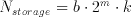 (5.1)
(5.1)
It must be noted that the storage for each bitplane will be identical, resulting in
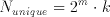 (5.2)
(5.2)
unique storage cells. These two expressions clearly show that regardless of the storage method a memory based solution is not very efficient for large values of m. Yet for a simple building block, large values of m are not needed. Even values of m are also not very practical as most convolutions used in DSP algorithms need the data point plus an equal number of neighbours, commonly resulting in a matrix of odd dimensions. Table 5.1 compares the amount of memory to the number of multiplications (assuming k=10) for selected values of m.
Table 5.1:Number of operations.
m            N-unique    8x8 Multiplications

3               80                 3
5              320                 5
7             1280                 7
In this work, m=5 was found as a more reasonable candidate as it has a relatively small memory requirement which is large enough to justify the peripherals associated with the storage elements. At first sight, the amount of computational complexity that the storage replaces may not seem significant. Multiplication is one of the most demanding and area consuming operations in the digital domain. Aries, as an example, uses m=5 and the storage elements can deliver the result of 5 multiplications in 10 ns, in a technology where a well designed Full Adder has a delay of about 1 ns. The same performance can only be achieved by the utilization of at least two (or more) multiplier blocks. Moreover the delay of the storage elements is independent of the coefficient dynamics, that is to say a result of any bit length will be delivered at the same rate as the 10-bit result. This allows for optimization in the bit-length, by which the delays of all pipeline stages can be carefully balanced to match the speed of storage elements, as increasing word lengths accounts for increasing processing in the subsequent combinational adder stages.
It is a known fact that the flagship of integrated circuits development is the realization Random Access Memory devices. Current technology is often referred in terms of storage elements per chip (such as 1 G-bit technology). Yet much of these advanced technologies are not available for common digital designs and large on-chip memories are not desirable, mainly because of their area requirements.
For small and medium scale storage within the constraints of conventional digital VLSI technology two practical solutions exist:
The most important advantage of the register array, which basically consists of an array of D-type flip-flops, is that the designer can safely use standart cell elements to generate the register array, completely avoiding the time-consuming full custom design effort. Most of the modern synthesis tools support these arrays and many contemporary designs include relatively large amounts of such structures. But the register array design also has several disadvantages:
 Figure 5.1: 2 x 2 SRAM array compared to 4 x 1 DFF array.
Figure 5.1 clearly shows the difference in silicon area. Even without any associated connections and peripherals, the full custom realization of a 2x2 Static-RAM ( ~1000um^2) occupies less than one sixth of the area of the registers (~6500um^2).
Although the advantages of using a RAM block is clear, it requires much more design effort than the standart cell based solution. Some semiconductor foundries have tools to automatically generate RAM blocks, while some others have services for commercial products (in which practically the foundry employs a RAM design engineer). In the case of Aries, the chosen semiconductor foundry Austria Micro Systems (AMS) did not have a RAM generator, so the RAM cells had to be designed in full custom.
Although inherently Dynamic RAM (DRAM) circuits have a much higher density, their design is much more complicated (state of the art DRAM designs rely on a broad range of technology enhancements which are not common in normal digital CMOS technologies), requires more sophisticated clocking and is usually slower than Static RAM (SRAM) circuits.
 Figure 5.2:General SRAM structure.
A generic SRAM carray and its peripheral circuitry are shown in Figure 5.2. The SRAM array consists of a dense two-dimensional arrangement of the actual storage elements. For small memories it is possible to store one word of data in a row (for larger memories one row holds several words of data). All cells in one column share the same input signals (called the bitlines). Prior to read or write operations, the bitlines are charged to a known value by the pre-charge circuits. The row decoders are used to select one row in the array. The storage elements in the row are connected to the common bitlines and either the value within the cell is sensed (read) by sense-amplifiers or is overwritten by write circuits depending on the mode of operation. For large memories, an additional column decoder is used to select the desired word within a row.
A simple CMOS-SRAM cell consists of two cross coupled inverters and two access transistors connecting these two inverters to complementary bitlines.
 Figure 5.3: Basic SRAM cell.
The two switches in 5.3 are simple nMOS pass-transistors. A so called wordline controls these pass-transistors. As long as the pass transistors are turned off, the cell retainsone of its two possible steady state.
A read operation from this cell is performed by pre-charging the bitlines to a known value (e.g. VDD) and enabling the wordline. As during any read operation only one row can be active (the row decoder guarantees this), each column (bitline) can be modelled by a capacitor representing all the parasitic capacitance of the bitline and the input capacitance of all the access transistors. Figure 5.4 shows the pre-charge circuitry and the simple SRAM cell itself, together with the column capacitances.
 Figure 5.4: Equivalent SRAM cell during Read and Write operations.
Depending on the content (i.e., the state) of the cell, one of the bitlines will be pulled down by the nMOS transistor of the inverter with the logic "0" state, while the other bitline will remain at VDD.
Figure 5.5 shows the simulation results of two consecutive read operations. The nMOS transistors of the simulated RAM cell have dimensions of W=3um and L=0.8um while the pMOS transistors and the access transistors are minimum width transistors, having dimensions of W=2um and L=0.8um. The parasitic bitline capacitance is modeled to be 1pF. The first Read Cycle starts at 160 ns with the activation of the wordline. The stored information is a logic "1", bitline rises to VDD while bitline' is pulled down by the second inverter. Notice that the bitline is not pulled down completely (in fact it only reaches 4 Volts) but that is enough for the sense amplifier to operate correctly. The second read operation starts at 180 ns with the activation of another wordline (not shown, which in fact is just the inverted first wordline). This time the stored information is a logic "0" and the switching of the bitlines can be seen clearly.
 Figure 5.5: Simulated SRAM read operation.
A write operation is pretty similar in nature to the read operation. Again the cell is accessed with enabling the wordline, but this time the bitlines are driven to a known state by the write circuitry. This write circuitry is designed to have a stronger current driving capability than the pre-charge and storage cell circuitry, and as a result the bitlines are driven beyond the inversion thresholds of the inverters within the SRAM cell.
 Figure 5.6: CMOS SRAM Write operation.
The plot in Figure 5.6 is a snapshot of a simulation used to verify the functionality of the RAM design. The first three strips are the control signals. Write enable signal activates the write mode, Wordline selects the rows to be accessed and the Data is the value to be written to the selected cell. The voltages of the bitplanes is plotted next followed by the voltages within the SRAM cell. (the inputs of the two inverters). The simulation snapshot displays consecutive write and read cycles. The first write cycle starts at 220 ns. A logic "0" is written to a cell within the column which is not the cell that we are concentrating. At 240 ns. a logic "1" is written into the cell. The Wordline goes high indicating a write to the cell we are observing. Notice the bitline swing for the write operation. Also the last two strips clearly show the switching inverters. A new value has been written. There is a read cycle starting at 280 ns. At 300 ns our cell is accessed for a read operation. Notice the relatively low bitline swing and the perturbation on the inverter. It is clear that a perturbation as high as the threshold voltage of the nMOS transistor may cause the inverter switch state and destroy the content of the cell. Kang and Leblebici [19] give a conservative analytical expression for the sizing of access and pass transistors to prevent overwrite during read.
 (5.3)
(5.3)
Substituting the values for the AMS 0.8um process VDD=5V and Vt,n=0.75V we get.
 (5.4)
(5.4)
The simulation shows a second write operation starting at 340 ns. At 360 ns logic "1" is written to the cell activated by the Wordline .
To achieve a higher RAM density, Aries uses dual port RAM cells. As each port must be able to access the cell independent of each other the basic access lines Bitline, Bitline' and Wordline need to be duplicated. Two more pass transistors are added to control access of the second port (See Figure 5.7).
 Figure 5.7: Dual-Port CMOS SRAM cell schematic.
An efficient layout for the basic cell is the key point of any dense RAM circuit layout. There are a few important factors to consider when designing a custom cell like this:
 Figure 5.8: Layout of the optimized Dual-Port CMOS SRAM cell.
Figure 5.8 gives the basic Dual-Port CMOS SRAM cell used within Aries. The basic cell measures 30.2um x 19.2um.
A very simple pre-charge circuit is used for the realization of the RAM. Unlike many SRAM designs, the SRAM in Aries does not use clocked pre-charge circuits. The RAM is targeted to operate at clock speeds of up to 100 MHz. A clocked pre-charge circuit would have needed a very accurate and complicated clock timing. The schematic of the static pre-charge circuit structure can be seen in Figure 5.9
 Figure 5.9: Pre-charge circuit schematic.
The pMOS transistors driving the bitlines have width of 6um , all the other transistors have dimensions of 2um. While providing a very simple column pre-charge mechanism, this structure also has some drawbacks:
The most important is that as there is a constant pre-charge voltage in the bitline, any effort to pull the bitline down must fight against this pre-charge circuit. One possible remedy would be to use minimum-size pMOS transistors in the pre-charge, but this is not feasible as a fast recovery is required to pull the bitlines from their low states to their high states. A weak pull-up would result in a slower response time in read access. On the other hand, the write operation needs to pull down the bitline even further, in order to be able to switch the internal inverters. A relatively strong write circuit easily accomplishes this task. This in turn has another negative effect. After any write operation one of the bitlines is pulled down to a relatively low voltage level. Thus, a subsequent read operation may under certain circumstances overwrite the content of the cell. Fortunately, this is not a major issue, since write operations are only required to update the weights; therefore, the write timing is not critical. In Aries, a write operation must be followed by an idle state (to help recover the bitlines) prior to a read operation. This restriction does hardly effect the operation of the circuit.
The main issue in the RAM design for Aries was the speed of read operation. The sense amplifier is the most important block that dictates the speed of read operations. The sense amplifier was developed by B. Aksoy [20]. A number of different architectures were evaluated. Finally, a two stage amplifier with a cross-coupled pMOS amplifier as the first stage and a conventional differential amplifier as the second stage was found to give the best performance. Figure 5.10 shows the schematic and the transistor sizing of the sense-amplifier circuit. Detailed evaluation and simulation results of this two-stage sense amplifier can be found in [20].
 Figure 5.10: Schematic of the Sense Amplifier.
The write circuit is a simple differential stage that is driven to saturation by Data and Data'. Two pass transistors and the current source for the differential amplifier is controlled by the Write signal. Figure 5.11 shows the schematic of the write circuit together with the sizing of non minimal transistors.
![[ZOOM]](PIC/mag.gif) Figure 5.11: Schematic of the Write circuitry.
Figure 5.11: Schematic of the Write circuitry.
A typical RAM circuit consists of an array of RAM cells that are arranged in rows and columns. The RAM can be laid out so that each row holds exactly one word of data, which for most RAM designs would generate blocks with dramatic aspect ratios that are totally unacceptable for efficient design both for their awkward geometry and the parasitics associated with especially the very long bitlines, not to mention the complicated decoder structure. For these reasons, RAM's are designed to contain more than one words in a row, with a two stage decoding process: First the row decoder selects the row of interest and than column decoders chose the required word from the selected row. Aries however required, only 32 different values for 8-16 bit data words (the exact word length was not chosen to be 10 at the beginning of the design). It was therefore possible to make an array without column decoders. The RAM array used, has an aspect ratio of 2:1 which is totally acceptable.
 Figure 5.12: Row decoder schematic.
Five address lines are necessary to decode 32 individual rows. For the design of Aries a two stage decoding structure was used. Figure 5.12 illustrates the decoding circuitry. The box on the top is the first stage decoder (pre-decoder). Please note that the block in the figure is not logic optimized and contains a number of redundant blocks. The block diagram represents the actual logic elements realized on the layout (the AND gate as an example is realized by a combination of NAND and NOT). The local inverters on the eight blocks are used to generate the complementary signals where needed and thereby reduce the number of vertical wires in the decoder.
There are two problems associated with writing to the RAM blocks:
Both of these problems can be addressed with relatively low design effort. For the first problem a very simple state machine as shown in Figure 5.13 can be used to generate the idle times. The circuit in the Figure 5.13 generates synchronous read and write signals depending on the state of "en".
 Figure 5.13: Read-Write state machine.
Aries uses a 2:1 multiplexer to achieve time domain multiplexing. A 3:1 multiplexer can be used to account for the write state where the address lines are supplied externally. As an alternative, a simple counter could be added in to the design to generate the addresses during a write cycle. These issues are discussed in Section 7.2.1
The layout of a single RAM column has evolved considerably during the design process. Figure 5.14 compares the initial floorplan to the final floorplan.
 Figure 5.14: Floorplan of the RAM column.
The initial floorplan tries to take advantage of the symmetric nature of the dual port architecture in which sense amplifiers and the pre-charge circuit of the other port is placed on the ends of the blocks. The first row of the RAM will always contain the value 0. A special cell consisting of this "zero-RAM Cell" and the write circuit was designed. This cell also switched the order of the bitlines which enabled using the same pre-charge and amplifier circuits. Although the idea is appealing at first sight, it creates a few additional problems:
The final floorplan has the write circuitry on one end of the block while two read ports are on the same side. This minimizes the routing for the next adder stages. The routing of the outputs requires ten Metal-2 busses to be placed after the sense amplifier block (as there are ten outputs). It was possible to place the pipeline registers underneath these busses, which saved a significant amount of silicon area.
 Figure 5.15: Floorplan layout of the complete Dual-Port SRAM. Detailed layout
of the circled area is shown in Figure 5.16.
Figure 5.15: Floorplan layout of the complete Dual-Port SRAM. Detailed layout
of the circled area is shown in Figure 5.16.
Figure 5.15 shows the complete layout. A close-up (marked with the circle on the complete layout) can be seen in Figure 5.16. The closeup shows parts of the first stage and second stage row decoders, the RAM cell array, the pre-charge circuit, the sense amplifier as well as the pipeline registers underneath the output bus. (the Metal-2 lines are drawn only as outlines as otherwise they would obstruct the view to the cells completely).
The layout of a single RAM block consisting of two separate address decoders, 32 rows of 10 Dual port SRAM cells, all the associated sense amplifier, write, precharge circuitry and the pipeline registers occupies an area of 390um x 815um (0.32mm^2). With these dimensions the RAM block is by far the most area consuming of all the Aries blocks. This was already predicted in the pre-design floorplan shown in Figure 4.3.
 Figure 5.16: Close-up of the Dual-Port SRAM layout (area highlighted in
Figure 5.15).
Figure 5.16: Close-up of the Dual-Port SRAM layout (area highlighted in
Figure 5.15).
A systolic structure is made up of an array of identical basic processing elements with same type of (similar) connections. The name systolic adder is actually misleading for this particular adder used within Aries. The name comes from the earlier adder design used within the Taurus architecture, where the partial results of all eight bitplanes were shifted and added in a single structure consisting of eight adder rows of five adders each (See Figure 3.6). In the present Aries architecture, the systolic adder is required to shift-add four numbers in each cycle, as a result of time multiplexing. Yet we have retained the name of this block, since the essence of the operation has not changed. This section will give an architectural overview of the designed adder. A detailed analysis discussing the design methodology will be presented in Chapter 8.
The algorithm in Aries requires that four numbers corresponding to the partial sums of bitplanes be added in one cycle. This operation can be summarized as:
 (6.1)
(6.1)
The multiplication with a power of two represents a shift-left operation. Symbolically this can be expressed like in Figure 6.1.
 Figure 6.1: Symbolical representation of the shift-add operation used in Aries.
As no general building blocks for the addition of four binary numbers exist readily, this operation must be broken down into a simpler form so that it can be calculated with the basic CMOS building blocks. For the addition of more than two binary numbers (multi operarand addition), two different structures are commonly used [5]:
 Figure 6.2: Multi-operand adder array with carry propagate adders.
Figure 6.2 shows the basic structure of a multi operand adder array which is constructed with carry propagate adders. This is called carry propagate because the carry from each adder is propagated directly to its neighbour. Only the sums of the adders within a row are passed to the next stage. The carries of all stages are evaluated with additional adders. The main disadvantage of this is the heavily serial nature of the operation. A worst case vector may cause the final result to be delayed more than m*n adder delays in an m x n adder array. A detailed analysis of the carry-ripple effect that causes this problem will be given in Section 6.1.2.
The carry output bit of a FA is by one order more significant than the sum output bit of the same adder. This is the reason why the carry is propagated in the carry propagate structure. It can be done differently though: In the carry save structure, the carry is saved, it is passed diagonally of the adder that is left to the adder that gets the sum output. This scheme is illustrated in Figure 6.3.
 Figure 6.3: Multi-operand adder array with carry save adders.
Notice that the last stage in the figure is in fact another carry propagate adder. The carries are saved until the last operation, which leaves two vectors; one consisting of the sum and the other of the carries of the previous operations. Needless to say, these two numbers have to be added. If the simple carry propagate adder is used as the last step the worst case delay will be m+n for an adder array of the dimensions m*n. This can even be enhanced if a faster adder is used as the final adder.
The most basic addition block that is used is the half adder. The half adder has only two 1-bit inputs, A and B, whose Sum can be calculated by a simple XOR operation. The Sum output is sufficient to express the sum of two 1-bit numbers for three out of four possible inputs. The sum of A=1 and B=1 can not be expressed by a single bit and a result with a higher significance than the Sum is required. This result is known as the Carry-out which states that an overflow has occurred.
The 1-bit FA is an enhanced half adder circuit having an additional Carry-in signal, which enables it to be cascaded with other adders and therefore is commonly used as a basic building block for generic adder arrays. The truth table of the FA is given in Table 6.1. (The truth table of the half adder corresponds to the first four entries in the truth table where Carry-in=0)
Table 6.1:Truth table of 1-bit FA.
Carry-In  A  B    Carry-Out  Sum
    0     0  0        0       0
    0     0  1        0       1
    0     1  0        0       1
    0     1  1        1       0
    1     0  0        0       1
    1     0  1        1       0
    1     1  0        1       0
    1     1  1        1       1
As the FA is the most widely used structure in a wide range of computationally complex functions, a significant amount of research effort was made on the realization of efficient adder structures. A quick glance to the truth table clearly reveals a classical XOR behaviour. XOR type functions typically have difficult CMOS realizations. A number of different realizations of FA's have been published [4,21,22,23,24] A well known CMOS FA structure was chosen in Aries since this adder is one of the most compact, robust and fast FA alternatives. The detailed design of a high performance FA cell, based on this adder, will be discussed in Section 8.3.2. The schematic of the adder and the transistor dimensions are shown in Figure 6.4.
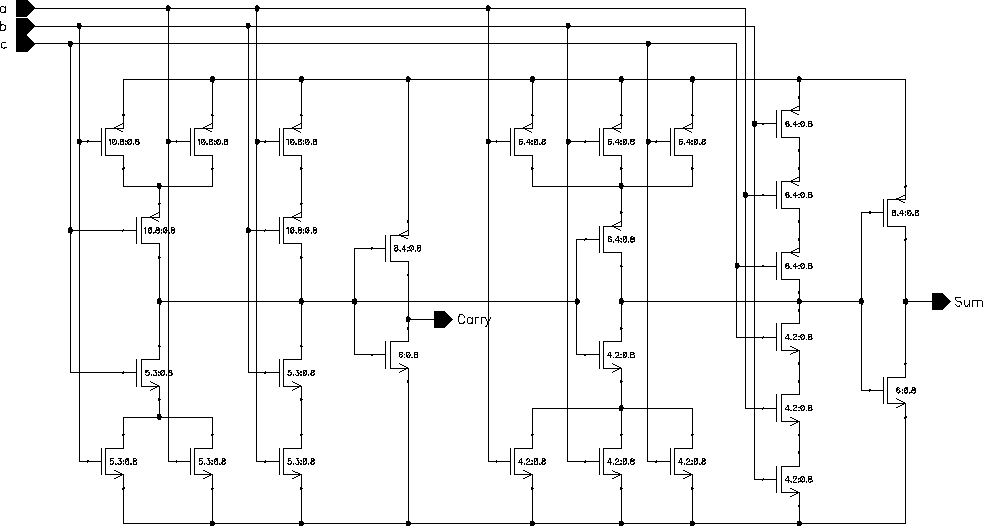 Figure 6.4: Circuit schematic of the CMOS FA.
Please note that in this implementation, Carry' is used to generate Sum; as a result the Carry signal can be generated before the Sum signal.
A total of n 1-bit FA's can be used to add two n-bit binary numbers (to be more precise n-1 FA's and a half adder, as the first addition would normally not have a Carry-in. This arrangement of FA's, where the Carry-out signal of the FA is connected to the Carry-in signal of the FA that adds the next significant bits, is known as the Ripple Carry Adder. The generic arrangement of the ripple carry adder is given in Figure 6.5.
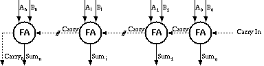 Figure 6.5: The Ripple Carry Adder.
Compared to all the known n-bit binary adders, the ripple carry adder is the most compact solution. It requires a small number of operational blocks (1 bit adders) and has a minimum routing overhead, as only the the Carry-out signals have to be connected to the Carry-in signals of the adjacent blocks. In a well designed layout of a FA circuit this connection can be made by simple abutment, which makes the design of the n-bit adder extremely simple.
The main drawback however, is that this realization is also the slowest parallel solution available. Although the adder accepts data in parallel, the operation is inherently serial because the addition of the i.th bit needs the Carry-out of the (i-1)th bit for the correct result. Starting from bit 0, the actual Carry is generated and rippled through all the stages to create the final result, hence the name ripple carry adder. The worst case scenario is when the carry of the first bit causes all the Sum bits to change. The delay for this operation is roughly expressed as n FA delays.
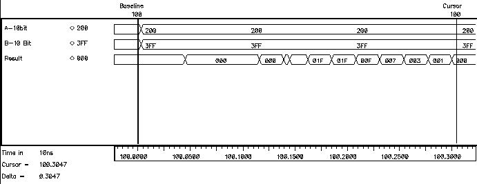 Figure 6.6: Simulated ripple effect in a 10-bit Ripple Carry Adder.
The behavioural simulation of a 10-bit Ripple Carry Adder in Figure 6.6 shows a worst case where A=(00 0000 0001) and B=(11 1111 1111) are added. All adders except for the adder of the least significant bits produce Carry-out=0 and Sum=1. Carry--out is available from the first adder (which in this case was at logic "0" prior to the addition) at the very first instant. As a result of the addition of the least significant bits (both of which are logic "1") a Carry-out=1 signal is generated by the first FA . With the arrival of this new (updated) signal the second FA starts calculating the correct result, generating another Carry-out=1 which in turn effects the third and all the subsequent stages. The carry generated by the first adder ripples through all the stages, causing subsequent transition of the sum bits. This is clearly visible in Figure 6.6.
Although it is true that for a worst case situation the carry will have to pass through a total of n adder stages, the associated delay is not exactly equal to n FA delays, as the Carry-out signal, for most efficient realizations of a FA, is calculated in advance of the Sum output which makes the overall delay shorter than expected. It is also easy to design a FA that is extremely fast for a single, given worst case situation (with far worse responses for other situations). Examples of this misleading approach are present even in the most known literature [21]. There are detailed analyses of the delay of the Ripple Carry Adder in the literature [25], but for first order estimation, the aforementioned worst case delay approximation of n FA delays is a solid measure.
One of the most serious drawbacks of ripple-carry adders is that: the delay scales linearly with the bit length, making adders operating on bit lengths larger than 16 rather in effective. A common philosophy in the microelectronic design is that in most cases silicon area can be traded off in order to get achieve higher speed. Addition proves to be no exception for this philosophy. A number of methods including, the carry skip adder, carry select adder, conditional sum adder, carry increment adder and the more general carry lookahead adder have been proposed. All of these methods are based on pre-determining the carry signal of a number of stages before the Sum of the previous stages is available.
The parallel prefix adder [5] is a universal adder architecture that covers all of the known parallel adder structures described so far. The addition is described in three distinct steps:
Let A and B describe the two input signals that are associated with each stage. Two special signals are extracted from the inputs in preprocessing: propagate (p) and generate (g) signals. These two signals are said to describe how the Carry-out signal will be handled. A Carry-out could be generated within the block or the existing Carry-in signal could be propagated to Carry-out. These signals can be easily obtained from the available inputs as:
 (6.2)
(6.2)
 (6.3)
(6.3)
The i.th carry signal, Carry(i), can easily be expressed as:
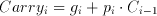 (6.4)
(6.4)
Likewise the i.th sum, Sum(i), can be calculated by:
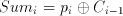 (6.5)
(6.5)
This is the task of the postprocessing step. This leaves only the Carry Propagation (Carry Lookahead) problem that needs to addressed. The carry propagation problem can be expressed in terms of a so called prefix problem where for a set of binary inputs (x(i):i=0,1,2,..,n) the outputs (y(i):0,1,2,..,n) are defined by the help of an associative binary operator Delta as:
 (3.3)
(3.3)
 (6.7)
(6.7)
The most important factor in this expression is that the Delta operator is associative:
 (6.8)
(6.8)
This sort of hierarchical organization brings in sub products which can be denoted as: Y^k(i:j), where k is the level within the hierarchy and i and j define the range that this sub product covers. For the carry propagation problem let us define the sub-product couple (G,P) such that:
(6.8)
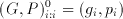 (6.9)
(6.9)
Where the desired
 (6.10)
regardless of the number of levels necessary to cover the range i:0. Given the two adjacent ranges a and b, the Delta operator performs the following logical operation:
 (6.11)
 (6.12)
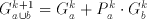 (6.13)
These equations reveal the following:
The graph representation of this problem provides a much clearer view of the algorithm. Two main symbols are used in the graph representation of prefix algorithms are given in Figure 6.7.
 Figure 6.7: Two main blocks of prefix algorithm graph representations.
As a simple example, let us express the Ripple Carry Adder structure as a prefix problem. Figure 6.8 shows a prefix graph representation of a 16-bit Ripple Carry adder.
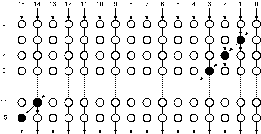 Figure 6.8: Prefix graph representation of a 16-bit Ripple Carry Adder.
With the figure of the Ripple carry adder in mind we can easily define some performance measures for prefix adders:
The Sklansky parallel prefix algorithm is one of the fastest adder architectures, the graph representation is given in Figure 6.9.
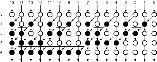 Figure 6.9: he graph representation of Sklansky Parallel Prefix Adder.
The main problems in the Sklansky Parallel Prefix Adder is that some nodes have pretty high fan-outs. Another alternative could be the Brent-Kung Parallel Prefix Adder which is shown in Figure 6.10.
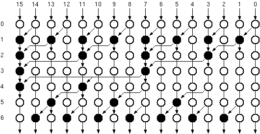 Figure 6.10: The graph representation of Brent-Kung Parallel Prefix Adder.
The Brent-Kung Parallel Prefix Adder is slower than the Sklansky Parallel Prefix Adder, but has less processing nodes as well as a much lower maximum fan out.
A generalized filter architecture must be able to cope with positive as well as negative coefficients. It is true that the hardware itself does not make distinctions according to the content of the data, thus performs the same operation regardless of the 'defined signs' of the operands. The problem however lies on the range boundaries of the number system used. The Two's Complement representation of negative numbers require a fixed data-length for proper operation. This accounts for extra complexity in shifted addition circuits where all operands have the same bit length but are shifted with respect to each other. The missing digits to the left of less significant operands have to be completed according to the sign of the operand. Luckily, this problem is easily solved as the last digit of any operand can be replicated to fill in the missing digits. A simple structure shown in Figure 6.11 controls this replication operation Aries, to enable a higher dynamic range for coefficients that consists of positive numbers only.
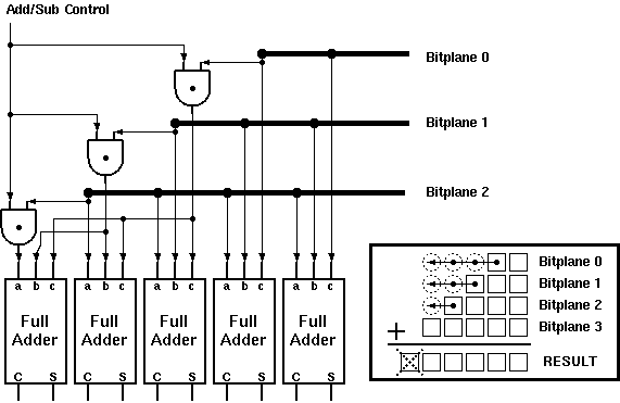 Figure 6.11: Adder Subtractor enhancement for the Systolic Adder.
The Carry Save Adder structure discussed earlier is the faster alternative for the Multiple Operand Adder used in the Systolic adder block. An operand bit length of 10 was found to be adequate for the design. As the capability to operate on negative numbers is also desired, the adder-subtractor enhancement discussed earlier was added to fill-in the missing digits. As a result of the negative number processing capability, the Carry-out of the whole block can safely be ignored which simplifies the design to some extend. The overall schematic of the Systolic adder is given in Figure 6.12.
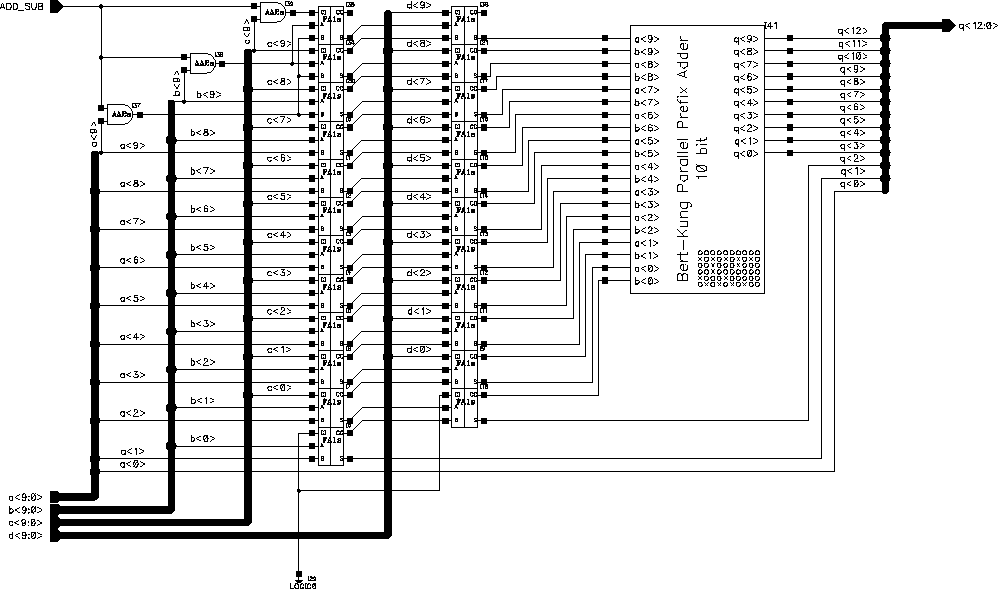 Figure 6.12: Schematic of the Systolic Adder.
The traditional Ripple Carry Adder scheme to calculate the final result from the two Carry and Sum vectors was replaced by a (modified) 10-bit Brent-Kung type Parallel Prefix Adder. It differs from a standart 10-bit adder in that the last Carry-out signal is not required and the carry propagate block is the same of that of a 9-bit adder. The general schematic of the modified Brent-Kung Parallel Prefix Adder is given in Figure 6.13.
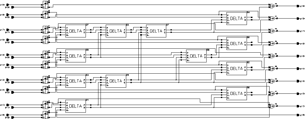 Figure 6.13: Schematic of the modified Brent-Kung Parallel Prefix Adder.
Please note that on both of the blocks the last Carry signals are left unconnected. The preprocessing blocks can be realized by simple half adders and the postprocessing block is a simple XOR gate. The "Delta" block actually performs the operation given in Equations 6.13 and 6.14, for which the schematic is given in Figure 6.14.
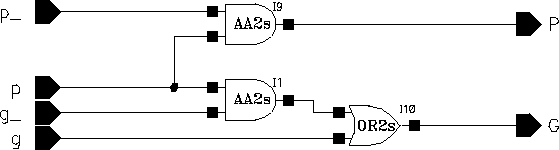 Figure 6.14: Schematic of the Delta block.
The final layout of the Systolic Adder including the pipeline registers is given in Figure 6.15. The adder dimensions, excluding the routing block at the bottom, are 320um x 300um in total.
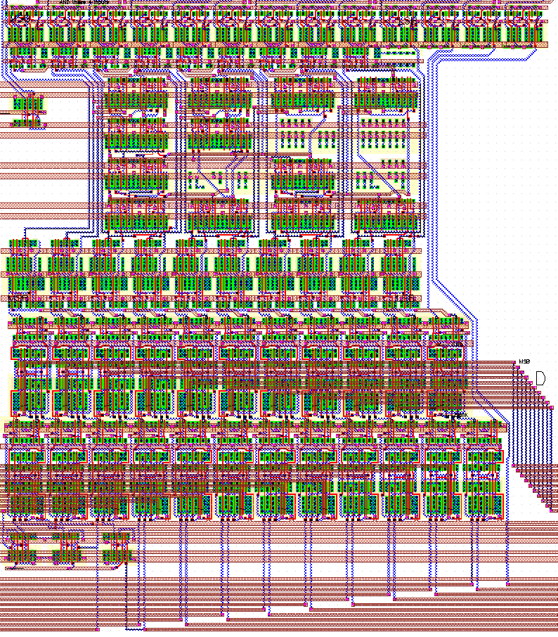 Figure 6.15: Final layout of the Systolic Adder.
Figure 6.16 shows a behavioural simulation showing the operation of the systolic adder. The four input vectors are named A, B, C and D respectively. The simulation starts with an initialization phase with all input vectors having a value of 0. At 10 ns four vectors are introduced to the systolic adder. All of these numbers are interpreted as positive numbers (operation mode is unsigned) and the result is calculated. At 20 ns, the vectors remain the same but the operation mode is changed from unsigned to two's complement. The first two vectors A=(11 1111 1000), B=(11 1111 1100), are interpreted as negative numbers and have corresponding weighted decimal values of A=-8 and B=-8. The result of this operation is 0. At 30 ns the first two vectors are changed to positive values. The result remains the same even after the mode of operation is changed to unsigned, since all vectors have the same value irrespective of the operation mode. The vector set which is applied at 50ns provides an interesting result. Although during both of the operation modes the result remains the same, the nature of operation in both cases is different. For the unsigned operation mode there is an overflow while for the two's complement operation the result is indeed 0. At 70ns a similar case with different vectors is tested, this time there is no overflow and the result is displayed correctly.
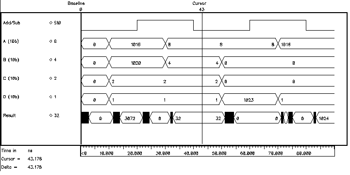 Figure 6.16: Behavioural simulation result of the systolic adder.
As described earlier in Section 4.1, Aries uses time domain multiplexing to simplify the hardware. While operating on 8-bit image data, the first 4-bit (nibble) is processed first and the result is stored in the accumulator. The same procedure is repeated for the second nibble. The accumulator adds this number to the stored result. As the second result is obtained from the higher-order nibble the result this time is actually 2^4=16 times the value it was calculated. Therefore, the second result has to be shifted by four digits to left prior to the final addition. The adder used in the accumulator is a 13-bit Brent-Kung Parallel Prefix Adder and was quickly designed by enhancing the Carry Propagation block for the additional bits. Once again a simple structure is used for negative coefficients compatibility. The schematic of the accumulator is given in Figure 6.17.
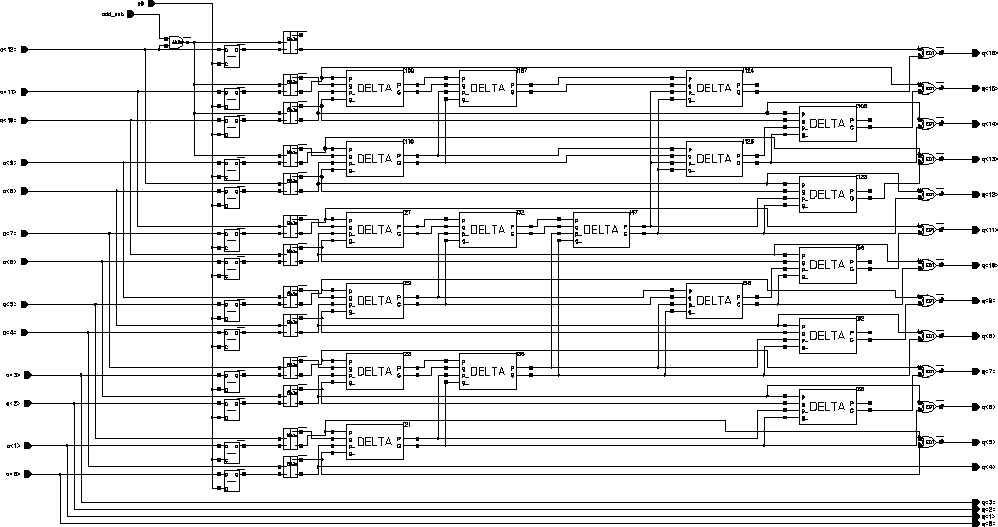 Figure 6.17: Schematic of the Accumulator.
The layout of the Accumulator block is shown in Figure 6.18, the layout dimensions are 340um x 200um in total.
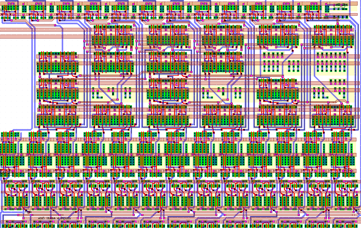 Figure 6.18: Layout of the Accumulator.
The registers within the accumulator block have different clocking signals. The systolic adder calculates a vector at every cycle, and the pipeline register samples this result at every cycle. The register within the accumulator block needs to sample the output of the pipeline register every two cycles when the result corresponding to the first four bits of data arrives. The result will be available at the end of next cycle. This result is sampled by the pipeline register following the accumulator stage. This timing is described in Figure 6.19
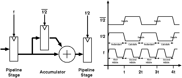 Figure 6.19: Block diagram and timing of the Accumulator.
This operation scheme has the disadvantage that some redundant calculations are made, specifically when the result from of the least significant 4-bitplanes are waiting to be sampled by the internal register they are shifted by four and summed up with the previously sampled sum of four least significant bitplanes. The result of this redundant operation is not sampled by the pipeline register. Needless to say this operation has no practical purpose and is totally redundant. To prevent the redundant calculations (and save power), a buffer stage could be used at the expense of silicon area, but as the redundant calculations do not produce any erroneous results this solution was not adopted for Aries.
To support negative numbers, the same solution that has been used in the systolic adder is employed. The last bit of the lower order operand is repeated to fill-in the missing bits. The only difference is that only one operand with four missing bits has to be filled instead of three operands with varying fill lengths. A simple AND gate is used to add a selective negative number processing capability.
The output of the accumulator is 17 bits long. In the earlier design phases it was decided that a barrel shifter be used to truncate this number to 8 bits. While this solution is ideal for a single block, it complicates the addition of partial results in the system level as outputs with different shifts have to be normalized before addition. Therefore, a unique high precision output is chosen. The least significant bit of the result is ignored in order to have a commonly used output of 16 bits. This truncation introduces some errors. Ignoring the least significant bit rounds positive numbers down while negative numbers are rounded up. This complicates the issue of correcting the error, since the error not only depends on the number system used but on the result as well. Table 6.2 summarizes all possibilities regarding the operands and the results and lists the corresponding error.
Table 6.2: Errors introduced by truncating the least significant bit.
Number System    1st Operand    2nd Operand    Result    Error

unsigned           positive       positive    positive    -.5
two's complement   positive       positive    positive    -.5
two's complement   positive       negative    positive    -.5
two's complement   positive       negative    negative    +.5
two's complement   negative       negative    negative    +.5
At first sight the error seems to depend solely on the result, but negative numbers are only a consequence of the different numbering system (two's complement). Any negative result in two's complement number representation format (a result with a MSB of logic "1") can be interpreted as a positive number in the unsigned number representation. The error caused by the truncation of the LSB will be different for both cases. Any rounding and/or truncation has an associated rounding error, but the error described above is an additional error to the conventional truncation error.
Since at any time all of the factors contributing to this error are exactly known (the result and the number system) it is possible to correct the truncation error. This correction can feasibly take place within the next stage, which is the Final Adder block. The overall Carry-In of the Final Adder can be used to compensate for the sign based rounding errors. Yet this approach was not used in Aries because the result of the accumulator can also be sent off-block by the output stage.
Figure 6.20 shows a simulation demonstrating the basic operation of the Accumulator. Both the input and the internal registers can be seen in the plot.
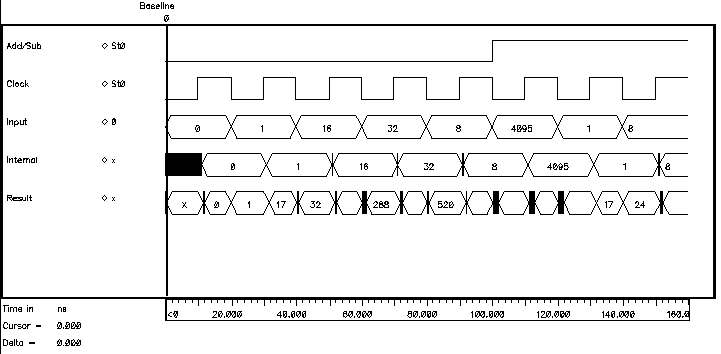 Figure 6.20: Simulation result of the Accumulator.
The output stage is not an internal block of Aries. It is intended to be used together with the final adder, to generate pipelined adder arrays to sum up the results of a number of Aries blocks. The details of combining several Aries blocks is discussed in detail in Section 7.3. The output stage determines the second operand of the Final Adder (the first operand of the Final Adder is always external), in which it decides:
The general block schematic of this stage is given in Figure 6.21.
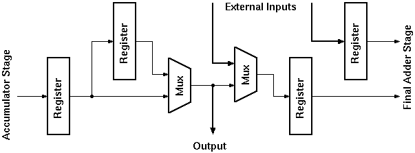 Figure 6.21: Block diagram of the output stage.
Two 2:1 multiplexers are used in the design. The first multiplexer controls the delay of the output while the last one selects either the internal data bus or an external data bus as the second operand for the final addition stage. Each of the multiplexers are controlled by a single bit giving four operational modes that are given in Table 6.3.
Table 6.3:Four different operating modes of the output stage.
   MUX-1          MUX-2                Operation Mode
Delay Select  Input Select   Accumulator Delay     Final Adder Operand
     0              0            No delay             Internal result
     0              1            No delay             External result
     1              0       1-pipeline stage delay    Internal result
     1              1       1-pipeline stage delay    External result
A very simple ripple carry adder structure is used as the final stage adder. The main purpose of this block is to allow cascading of Aries blocks to form a larger filter array. Since the output of the main Aries block is limited to 16 bits, a 16-bit adder structure is used within this block. Note that a simple ripple carry adder was used for the adder, as this block operates at half the speed of the internal adders. Initially the design of Aries consisted of a barrel shifter within the accumulator block which would provide 8-bit results. This solution was later given up to increase the resolution in the adder chains. Still, a simple ripple adder structure is sufficient to meet the speed requirements of the adder. The 16-bit sum of two operands has to be calculated in a pipeline stage within 20 ns which can easily accomplished by a ripple carry adder using the FA cell used throughout the design.
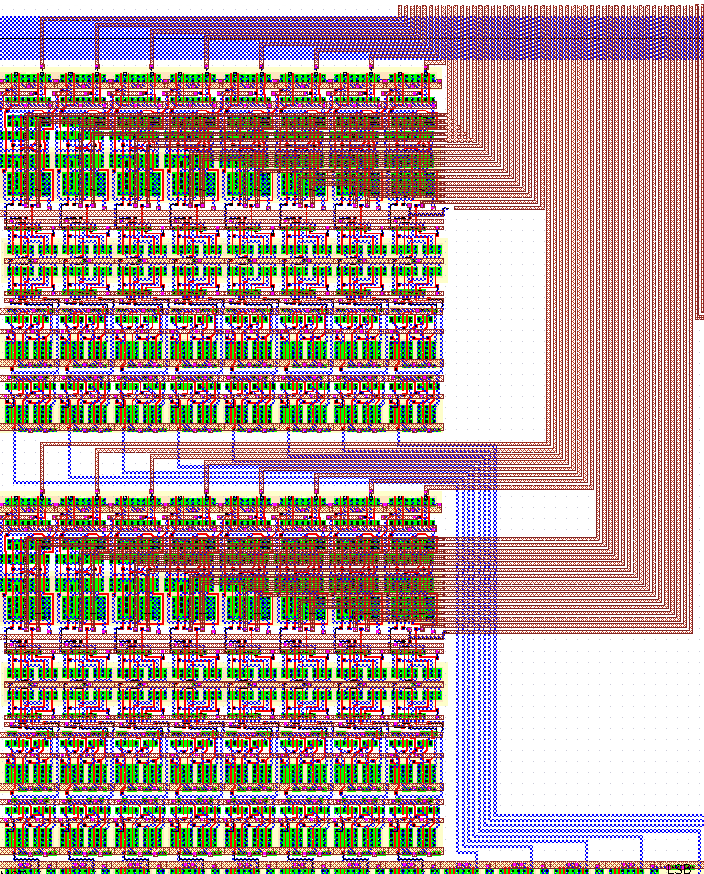 Figure 6.22: The layout of the output stage with the final adder.
The Figure 6.22 shows the layout of the output block with the final adder and all associated pipeline registers. The layout was designed and optimized for a 8-bit output stage in mind, and can not accommodate a 16-bit computation block. therefore the block is broken down to two 8-bit pieces. This scheme can be easily employed, as the ripple-carry adder used in the last stage can be broken down into two pieces without complicating the routing extensively (only the Carry-out signal of the last stage needs to be connected to the Carry-in of the subsequent stage).
The final layout of the Aries architecture can be seen in Figure 7.1. The layout occupies an area of 1.26mm x 1.13mm (1.425mm^2). Please note how closely this final layout conforms to the initial floorplan given in Figure 4.3. The lower part of the layout comprises of the two shift register blocks. the space between these blocks is reserved for clock buffers and SRAM read/write circuitry. The two Dual-Port SRAM blocks dictate much of the circuits size. Three stages of adders are placed in between these rows.
 Figure 7.1: Final layout of the Aries architecture.
Aries has two main operation modes: Initialization Mode and Computation Mode. The operation of Aries relies on pre-computed co-efficients that comprise the filtering kernel. Prior to computation mode these values have to be loaded into the RAM blocks. The Initialization Mode serves this purpose. The Computation Mode is the general operation mode where at each clock cycle a new data is read and the result in the current pipeline is send to the output. The Computation Mode can be interrupted by a Initialization Mode to update the co-efficients.
An Aries block is expected to operate mostly in the Computation Mode. The Initialization Mode is necessary to load the values of the co-efficients after the chip has been powered-on. The same mode can be used to update the values of co-efficients during normal operation. Intelligent adaptive filtering algorithms fine tune the coefficients during operation to obtain better results. The process of updating the coefficients will cause an interruption of processing, for some signals like images this would not be a real problem as most of the image signals have a blanking time where no actual signal is present. Figure 7.2 shows the general block diagram during the Initialization Mode
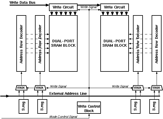 Figure 7.2: General block diagram during the Initialization Mode.
A single bit controls the mode of operation. The RAM blocks within Aries require an idle state between write and requests. The single bit drives the aforementioned (see Figure 5.13) RAM control block. This control block inserts an idle state after the first clock (the fast clock is used within the RAM blocks). All four RAM blocks within Aries need to have exactly the same information. As two dual port RAM blocks are used only two blocks need to be written. Once the write signal has been issued by the control block, the Multiplexers at the end of the shift registers select the same external address lines. The total control for the write operation has now been transfered to an external source.
The write operation is not clocked, any value in the write bus is written to the row addressed by the address lines. The circuit ensures that the total decoding and writing will take less than 10 ns. After all the co-efficients have been loaded the mode control bit can be changed to the Computation Mode value of logic "0". Figure 7.3 shows the timing of the Initialization Mode.
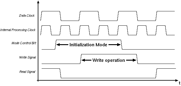 Figure 7.3: Timing of the Initialization Mode.
A simple external counter can be used to update all the coefficients within the Aries block.
For most of the time the Aries block is expected to run in the Computation Mode. This is the mode that actually performs the convolution. Only a few control signals have to be set for proper operation:
Aries is a fully pipelined design which causes a certain latency in the output (depending on the adder tree and the mode selections the latency may change). It must be noted that all five data registers must have valid values before the first value can be calculated. This initial value problem can be addressed in which the first value is fed five times to fill up all the registers with a known value.
Another important issue is that overflow within the internal adders is not propagated to the output. Overflows within the addition blocks (especially when two's complement number representation is used) can cause erroneous output. An overflow flag would not be of much use as there is no practical way to re-calculate the whole value (the pipeline will contain partial results for subsequent operations, that has to be cleared first). For fixed co-efficient applications the co-efficients can be chosen accordingly, to ensure that there is no overflow within the block. For adaptive applications the co-efficient dynamics can be kept within certain bounds (notice that the limitations will depend on the number representation system and in any case will cause only slight restrictions on the co-efficient dynamics).
Aries is designed as a basic building block to be used in the design of higher order 1-D and 2-D signal filters. A number of identical Aries blocks can be used to generate the desired kernel size. This section documents how a number of Aries blocks can be combined to form a complete filter. As 1-D kernels can be considered as a special case of a 2-D architecture (where y=0) this section only concentrates on the design of 2-D kernel structures. Figure 7.4 shows the general structure used to combine a number of Aries blocks.
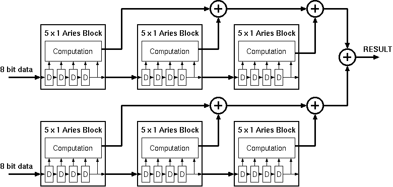 Figure 7.4: General structure used to combine a number Aries Blocks.
Each Aries block can be used as a 5x1 filter kernel. Using an appropriate number of blocks any size of filter kernel can be realized. Scaling in the Y direction is relatively easy, as the data in every row is independent of each other, it is enough to add a new data input line and repeat the structure used for X axis alongside the row. The results of different rows have to be added at the end. Scaling on the X axis is a little more tricky. The length of the kernel along the X axis actually corresponds to the number of subsequent samples that have to be processed. This time delay is realized by the input registers in Aries. At every rising edge of the clock a new data is read and the remaining data are pushed deeper in the shift register chain. To be able to scale in the X axis this pushed data has to be transferred to the next stage. Aries uses a separate bus to transfer the outputs of the shift registers to the next stage.
A design with n Aries blocks will generate n independent results each clock cycle. These results need to be added to form the final result. As these results are independent of each other, they can be added in any order. The final adders (see Section 6.4) within the Aries block can be used to perform this addition. Using a binary tree structure theoretically n numbers can be summed up using at most n-1 adders. As there are n Aries blocks, there are enough adders present to form a binary tree. For a binary adder tree with exactly 2^n operands it is possible to create a pipeline without any problems. Figure 7.5 shows an adder tree that adds up 17 results . Although still 16 adders are required for the operation notice that the result of block 17 is added to the combined sum of the first 16 blocks which are calculated in a four level adder tree.
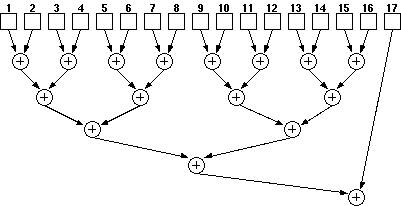 Figure 7.5: A binary tree adder for 17 numbers.
For a pipelined architecture this is not acceptable, as the result of the 17th block needs to wait for four adder delays. A pipeline structure would require that fouradditional delay elements be used for the result of the 17th block. This problem is solved by the output stage of Aries which is described in Section 6.3. This arrangement has two modes: one where the result is available directly and another one where the result is delayed by one pipeline stage. Both of these results can either be fed to the internal final adder or redirected to output. It can be shown that any number of operands can safely be implemented with this arrangement.
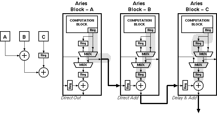 Figure 7.6: Three Aries output block configured for pipelined addition, block
diagram (left) and detailed schematic (right)..
Figure 7.6: Three Aries output block configured for pipelined addition, block
diagram (left) and detailed schematic (right)..
As a simple example let us consider the addition of three results, Figure 7.6 shows three Aries blocks and their output modes. Notice that all three modes are used in this arrangement. The only restriction of this methodology is that the output can only be delayed by one cycle. All these delays have to be introduced at the first level of the adder tree. To construct such an adder tree it is necessary to start from the last stage where a single adder will be used. The total number of operands are divided into two halves so that the result will be two equal numbers for even numbers and two consecutive integers for odd numbers. This process is repeated until blocks of either two or three operands are reached. Thenafter the arrangement shown in figure 7.6 is used for a three operand addition. If any three operand additions exist (which is the case when n is not a power of two), all two operand additions have to be delayed by one clock. This is accomplished by setting the delay on both of the blocks, which will pass the results through the additional pipeline register before the final adder.
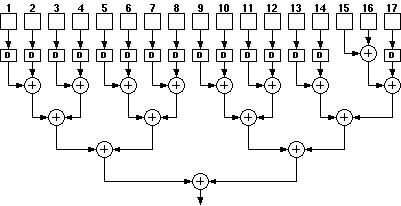 Figure 7.7: Fully pipelined binary tree for 17 operands using Aries blocks.
Figure 7.7 shows the arrangement for a pipelined 17 operand adder. On the first level there are 7 , 2 operand additions and only one 3 operand addition. As a result all of the operands of the two operand adder have to be delayed by one cycle. From the second level on it can be seen that all results can be calculated within the same clock cycle.
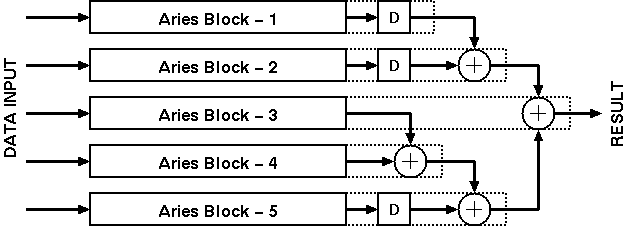 Figure 7.8:General arrangement of 5 Aries blocks to realize a 5 x 5 filter .
The general arrangement for a 5 x 5 filter would be like the one illustrated in Figure 7.8. Filters of any dimensions can be realized with the configuration shown. Another approach for building large filters would be to include a small RISC processor core to help programming the weights of all Aries blocks as well as add intelligent scaling algorithms for the results. The general block diagram of a large filter array that uses a RISC processor core is given in Figure 7.9.
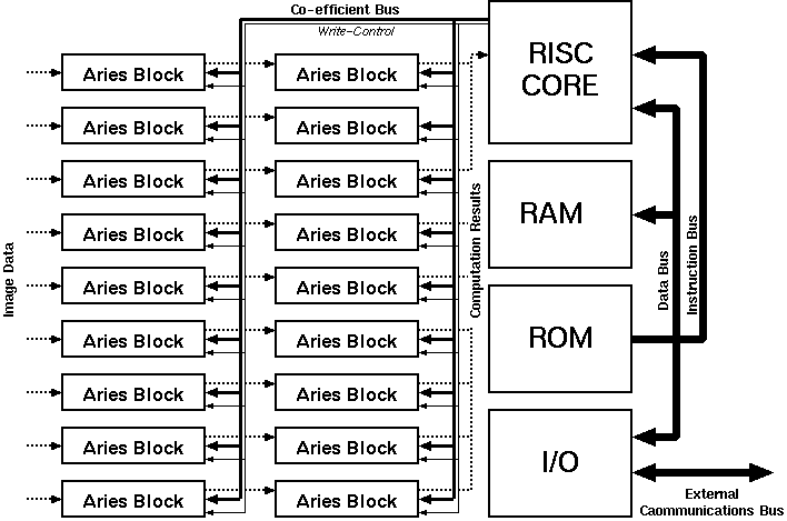 Figure 7.9: A large filter realization using Aries blocks with an embedded RISC
processor core to update weights.
Figure 7.9: A large filter realization using Aries blocks with an embedded RISC
processor core to update weights.
This section presents the design methodology used for the design of various blocks within the Aries architecture, with a specific focus on full custom design of high-performance arithmetic units.
A successfull design has to satisfy a number of performance criteria as described in a so called "design specification". A design specification typically describes and sets minimum/maximum limits for the following performance criteria:
and defines a set of functions that the finished design is required to realize. As long as these requirements are met the design is said to be successful. If the design specifications are set in a conscientious manner, there should be no need to further improve any of the performance criteria beyond the limits described by the specifications, especially since this improvement will typically be at the expense of extra design time. Thus, a design that could operate at faster speeds than the given specifications is not necessarily more successful than a design that works within the limits specified.
The increasing improvements in integrated circuit manufacturing technology have resulted in smaller and faster circuits to an extent where the parasitic interconnection delays have equalled the delays of the blocks they are connected to. As a result, the dominance of aggressive speed and area requirements tends to diminish in modern designs. The high integration trend is also followed at the system level where an ever increasing market for portable devices has emerged which has increasingly contributed to the power specifications of a design.
In the 1990's the design time has established itself as one of the most dominant factors in any circuit specification. Most companies that develop integrated circuits need constant enhancements in their product line to meet the constant demand of the market. If the design is not ready on time for the market, a product from another company may address the demands and as a result the design will have missed the market.
There are various methods for designing circuits, each with its own set of advantages and disadvantages. The correct methodology for a design is based on many factors like:
Integrated circuit design is the process of mapping a functional description of a problem on silicon so that it satisfies a set of performance criteria. The design methodology may concentrate on any level of abstraction defined within this process: From the design of actual layout masks to the high level behavioural description of the circuit. Recent literature on digital integrated circuits describe a number of distinct methodologies. All of these methodologies can be grouped into two mainstreams that differ in design philosophy:
The Top-down approach starts the design process from high-level, behavioural descriptions of blocks that will realize certain functions ,while in the Bottom-up approach the low-level elementary building blocks of the circuit are designed and combined to realize the desired function.
The logic synthesis methodology is a good example for the Top-down approach. Initially developed as a common language to describe the behaviour of digital blocks, the VHDL description of a digital circuit has soon become a widely used method for automatic synthesis of such circuits, based on a library of standart cells. This approach successfully shields the designer from the complexities of physical design and thus, speeds up the process. Yet, a number of issues such as carefull speed optimization and area minimization/management can not be addressed by a straightforward top-down design methodology.
Full-custom, mask-level design of elementary building blocks, on the other hand, is a good example of the bottom-up design strategy. This approach is also limited by the fact that the overall design complexity quickly becomes very difficult to manage in larger VLSI designs.
For most efficient results, the design of complex VLSI chips should employ a combination of bottom-up and top-down strategies which is also called the "meet-in-the-middle" approach.
Full Custom design is probably the most time consuming and detailed of all the available design methodologies. It comes at an enormously high price: costly design time. Any designer attempting to employ a Full Custom design methodology must be able to provide a satisfactory answer to the following question:
" Why do I have to design this Circuit (or block) in Full Custom ?"
The usage of this costly method must be fully justified. Most common reasons for employing a Full Custom design methodology include:
Full custom design gives the designer the freedom to modify every aspect of the design to increase the performance of the circuit. While more freedom in design parameters provides ground for more optimum solutions, it also complicates this optimization process considerably. A clear focus on design goals is of much more importance in Full Custom design than in any other design style.
Even for the most simple circuit (e.g. an inverter) with pre-set electrical parameters (such as the ratios of transistors), the designer will be confronted with a lot of options on:
The designer must be able to realize the significance of his/her decisions and maintain a continuous picture of the design status in his/her mind to be able to refine these decisions.
The design of a layout starts with the definition of the signal flow. The signal flow defines on which layer and in which direction all the input, output, clock and power lines will be laid out. This flow will give the basic guidelines for the actual design of the layout. A good signal flow minimizes the connections for the block and ensures an overall compact layout.
As a simple example let us consider the signal flow for a simple inverter that will be used to invert and/or buffer a 32 bit bus running vertically in Metal-1 in a double metal process. Figure 8.1 shows an example signal flow.
 Figure 8.1: Signal flow for a simple inverter.
The reasoning behind that signal flow is simple. The main aim is to buffer or invert the bus signals so the input must follow the direction of the bus and should preferably be on the same layer as the signal. Every cell will need power and ground connections, a different layer (Metal-2) is chosen to avoid intersections with the signal line. A narrow block is more desirable as this block will be repeated along the X axis. Figure 8.2 shows three different layouts for the inverter cell.
 Figure 8.2: Three different inverter layouts based on the signal flow shown in
Figure 8.1.
Figure 8.2: Three different inverter layouts based on the signal flow shown in
Figure 8.1.
Notice how many different solutions we can come up with for a design with fixed electrical characteristics and signal flow. The first layout in Figure 8.2 is what we can call a traditional design. The second layout has the same structure and still is in accordance with the signal flow (only the input is still in Poly not in Metal-1) the only difference is that the power connections have moved toward the center of the cell. The third layout is a radical approach, in an attempt to make a narrower cell. The third cell does not follow the signal flow exactly, as the power connections are in Metal-1 instead of Metal-2. Although at first sight this seems to be against the aforementioned signal flow rules, it is not a crucial infringement. In fact, the signal flow picture can be refined, noting that: ("It is also possible to use Metal-1 for the supply connections if layout three is used"). Notice that the wider pMOS transistor of the inverter in the third layout has been realized by a parallel connection of two small pMOS transistors.
At this stage, the third layout seems to be a better candidate, as the width of the layout is clearly less than the other two. Let us continue and try to build the inverter block.
 Figure 8.3: 32 inverters placed side by side.
Figure 8.3 shows four different arrangements of the inverters. The first row is a simple repetition of the first layout. It is the largest of all solutions with dimensions of 285um x 23.5um (6697.5um^2). This area can be reduced using the following trick: A close inspection of layout 1 (and layout 2) reveals that the VDD and GND connections of the layout is on the left. These connections can be shared between two adjacent cells by simply mirroring the second cell. The second row in Figure 8.3 shows the result. The combined-cell consisting of a normal and a mirrored cell is shown at the end of the row. Notice that the inputs are not evenly spaced on this row. The second occupies less than 80% of the area of the first row with dimensions: 225um x 23.5um (5287.5um^2). The third row is generated by using the second layout. This cell is very similar to the first layout and can use the same mirroring scheme. The inputs which were in Poly in the single cell however have a higher degree of freedom and are placed afterwards evenly on this row. Although the second and third rows have the same width, the base cell of the third row is slightly smaller and as a result the third row occupies less area than all the others 225um x 21.5um (4837.5um^2). The last row shows the placement of inverters from the third "narrow" layout. This row of inverters is by far the most narrow of all, but with the dimension of 190um x 30.5um (5795um^2) occupies more area than all but the first row.
Let us continue our example in which we develop a 32-bit parallel buffer, where each buffer element consists of two cascaded inverters. The layouts of three buffer rows based on three different inverter designs can be seen in Figure 8.4.
 Figure 8.4: Three different layouts of 32-bit buffers, based on the inverters
shown in Figure 8.2.
Figure 8.4: Three different layouts of 32-bit buffers, based on the inverters
shown in Figure 8.2.
The first row is generated with the first inverter layout and has dimensions of: 225um x 40.5um (9112.5um^2). The reason for the reduction in height is again a mirroring trick: The ground connection that was running at the bottom of the cell was shared between the first and second inverter. This required a small re-arrangement in the input and output pins. The second row uses the second layout and is slightly larger with dimensions of: 225um x 44.5um (10012.5um^2). The mirroring trick could not be employed here as the basic cell of the second row does not have common lines at the bottom or top of the cell. The third row is still the most narrow block but occupies more area than the two other rows: 190um x 61um (11590um^2). It seems that despite the overall larger area, Next we demonstrate that the area occupied by interconnection lines may also play a very important role. Figure 8.5 shows a 32-bit minimum width Metal-1 bus that is connected to a row of inverters, placed side-by-side. The area used to match the bus to the inputs of the inverters is almost twice the size of the inverter block, 55um x 190um (10450um^2) !
 Figure 8.5: 32-bit Metal-1 bus connecting to a row of inverters placed side-by-side.
Most of the time the signal connections and routing will have a high impact on the overall area. Especially for blocks that have large number of connections the area required for signal routing might be even larger than the active area itself. Following the example we can deduct some basic guidelines for the layout of basic building blocks:
A full custom designer actually designs the layout masks that will be used in the manufacturing of the chip. All layers in the process have some restrictions on their size, aspect ratio or separation, as a result of different physical, chemical, lithographic process limitations as well as electrical properties of the device. These rules are defined in design rules. Basically, the process manufacturer guarantees that the layers will be manufactured correctly only if these rules are followed.
Different processes have slightly different rules for their technology which makes it difficult to find unique guidelines for compact layouts. Depending on the technology, one or more of the following items (rules) may impose the most restrictive limits in a full-custom design.
nMOS-pMOS separation:
Two transistors of different characteristics
need to be manufactured on a common substrate in CMOS design. Depending
on the substrate type one, (or even both) of these transistors are
manufactured in a well that has the appropriate doping concentration.
As a result the pMOS and nMOS transistors usually need to be separated
by a large distance margin. Traditional cell design places all pMOS
transistors in a common well and all the nMOS transistors below an
imaginary line separating both regions. Generally speaking, all CMOS
designs have a large connectivity between nMOS and pMOS transistors.
In order to have a more compact layout, two or more of these pMOS-nMOS
rows could be stacked on top of each other. As pMOS-nMOS spacing is
more than the spacing between same-type transistors a common trick,
is to change the ordering of the rows (resulting in a nMOS-pMOS-pMOS-nMOS
configuration). Both of these alternatives can be seen in Figure
8.6.
 Figure 8.6: Two alternatives of nMOS-pMOS transistor placement in a cell: Traditionalplacement
where all pMOS transistors are grouped on top and all nMOS transistors
are grouped on the bottom (left), Stacked placement where alternating
rows of nMOS and pMOS transistors are placed on top of each other
(right).
Figure 8.6: Two alternatives of nMOS-pMOS transistor placement in a cell: Traditionalplacement
where all pMOS transistors are grouped on top and all nMOS transistors
are grouped on the bottom (left), Stacked placement where alternating
rows of nMOS and pMOS transistors are placed on top of each other
(right).
Substrate Contacts:
The substrate on which the transistors are manufactured
must be kept at certain voltage levels for proper operation, and in
particular, to avoid latch-up problems. An N-well (or substrate) in
which pMOS transistors are realized, needs to be biased at the most
positive voltage (VDD for example) while a P-well (or substrate) needs
to be biased at the most negative voltage (GND for example). The structures
that connect the supply lines to the substrate are called substrate
contacts. These contacts, depending on the technology, could require
a considerable area especially for small designs. A good solution
is to try to share these substrate contacts underneath the supply
connection with neighbouring cells.
Interlayer connections:
There are a number of conduction layers in
any technology (such as polysilicons, Metal-1 and Metal-2). These
layers are separated with insulating SiO2 layers. Any connection between
these layers requires a vertical link (hole) through the insulator
which are called via's (for inter-Metal connections) or contacts.
Both layers must cover this hole to a certain extent. Combined with
the width of the contact or via hole and the required extension, the
area needed to make a transition from one layer to the other can be
much larger than the minimum drawing widths of the conduction layers.
Similarly, making multiple connections between three or more layers
may result in severe area penalty, unless the technology allows stacked
via's. Additional problems arise when these contacts are required
to have a certain distance to other layers. For cell design, the basic
problem is to connect the terminals of a number of transistors. As
only Metal-1 is used for drain and source contacts, and all signals
to the gates must be connected to poly lines, almost all signals have
to be carried down to these layers. The restrictions might make using
other layers for intercell routing unfeasable.
Varying pitch of metal lines:
For a given technology, different Metal
layers may have different pitches (pitch = minimum repetition distance
of a layout pattern). Combined with the problems described for interlayer
connections, this would require that busses that are going to be routed
using these layers will have a pitch that is dictated by the pitch
of the widest layer.
45 degree routing:
The majority of automatic tools and algorithms
are based on orthogonal (i.e. x- and y-direction) connections only.
Yet, it is also evident that if signal connections could be made as
a straight line from one point to the other, the connection distance
and all associated parasitics would be minimized. Drawing structures
with free angles that conform to the design rules is an extremely
complicated task and the computational complexity for Design Rule
Check (DRC) programs increases to impractical levels. 45 degree routing
is a trade-off between these two extremes: for some connections the
connection distance could be much shorter and following rules is not
much complicated than the orthogonal rules. Most technologies allow
the designer to use 45 degree features, at least in the conduction
layers. While using 45 degree features could reduce the area of a
cell to some degree, it is not completely problem-free. Especially
for technologies where contacts and/or via's are not allowed to have
45 degree features, this technique is severely limited. Another interesting
aspect is that the area that has been saved by the 45 degree features
can (for most of the time) only be utilized by other blocks that also
have 45 degree features.
A typical Full Custom design cycle for a block starts with the circuit-level schematic of the design. Repeated transistor level simulations are used to satisfy all functional and electrical requirements for the block. The designer then draws the most efficient layout (which is expressed in terms of design time, area and speed). The electrical devices and parasitics are then extracted from this layout, which is simulated to see if the design goals were indeed met. The post-layout simulation is considered to be the most accurate verification of the design, prior to manufacturing, as it contains all the parasitic effects associated with the particular layout of the circuit. While these simulations are more detailed than the pre-layout simulations, the input data provided by the circuit extraction program which has some known limitations.
The extraction algorithms typically use very simple algorithms to measure the size of specific structures. The extraction of device parameters is no exception. Figure 8.7 shows three different transistors.
 Figure 8.7: Three different transistors with the same extracted parameters.
Even the most advanced extraction algorithms would extract these three transistors with the same parameters (W=18um, L=1um), as the algorithm simply calculates the overlap of poly line with the diffusion pattern. Yet, these transistors will have radically different behaviours in real life. The first transistor (left) is a proper 18um transistor where the channel current will flow strictly across the channel . For the second transistor (middle), the effective channel will be narrower and longer than the one that the geometry suggests Since the carriers (electrons) must travel a longer distance through the channel, following a diagonal path from source to the drain contact. The third example (right) shows another extreme condition. Here the majority of the current will flow in an effective channel that is much smaller. At any case, the actual electrical behaviour of these transistors will be quite different from each other, but the post-layout simulations will fail to reveal these differences and treat all three transistors the same.
The design of the circuit schematic is usually based on electrical requirements and is an optimization process. The most important tool during this optimization is the simulation. The result of the optimization is a schematic that has defined values for the active devices. The layout is then drawn to convert this schematic into an actual circuit.
The full custom design methodology gives the designer a great level of freedom during the design. This freedom should also be exploited during the conversion of a schematic into a layout. For example, it is not very efficient to draw many transistors of different size. This is true especially for transistors of the same type that are connected to each other. Attention must be given to reflect the dimensioning of the schematic as close as possible, but especially for digital circuits, there is no good reason for trying to stick to exact, pre-defined numbers.
The choice of the circuit schematic can be very important. For some common blocks there are many different alternatives with varying advantages and disadvantages. As an example, XOR and MUX type circuits are hard to realize in standart CMOS logic whereas in Pass transistor logic their realization is quite simple. A very interesting design style for efficient layouts is the branch based logic style [4]. The branch based logic style is a special case of the standart static CMOS designs where both the nMOS and pMOS block of the circuit are designed using parallel branches of series-connected transistors between the VDD (or GND) and the output node. An example circuit schematic comparing the Static CMOS logic to the Branch Based Logic is given in Figure 8.8
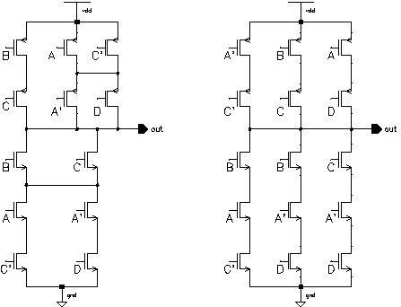 Figure 8.8: Schematic comparing the static CMOS logic to the Branch Based Logic.
Note that both circuits perform the same logic function
 (8.1)
(8.1)
At first sight the Branch Based logic realization (right) does not look like an optimum solution as it needs more transistors than the standard static CMOS (left) version. When we compare the layouts of both blocks shown in Figure 8.9, the advantages of the Branch Based Logic can be seen more clearly.
 Figure 8.9: Layouts comparing static CMOS logic to the Branch Based Logic.
The structure of the Branch Based Logic is very simple and does not have any exceptions. All blocks have a single power line and a single common output line. The most important property is that the diffusion region does not have any interruptions. The pMOS network of a Branch Based Logic realization is not the topological dual of the nMOS network, but it is very easy to calculate the two networks from a simple Karnaugh map as shown in Figure 8.10. Note that both the nMOS and the pMOS block functions are minimized strictly in the sum-of-products form.
 Figure 8.10: Karnaugh map for Branch Based Logic realization.
The nMOS networks is generated by using the sum of products representation from the Karnaugh map by selecting the "0" cubes. The pMOS network is selected by a similar way but the "1" cubes are selected, but as a pMOS transistor is turned on by a logic "0" on its gate, all the variables are inverted.
This section will discuss some aspects of the design of the Systolic Adder in detail to illustrate the design methodology employed throughout the design of the Aries architecture.
The first step after having a complete functional description is to come up with a functional schematic. The schematic given in Figure 6.12 was the first schematic designed to test different components, especially the final carry propagate adder. This gate level schematic is repeated in Figure 8.11 for reference. The whole schematic consists of standart cells and gives a good overview of the connections and complexity. The concept and some difficult test cases can be simulated to verify the functionality. The final carry propagate adder is designed as a separate subblock which can be replaced on the top-level schematic easily. The same schematic is also usefull while evaluating the post-simulation results and generating test cases.
Figure 8.11: Schematic of the Systolic Adder.
The basic building block of the systolic adder block is the one-bit FA, therefore an area efficient and high-speed FA cell is the key to the fast systolic adder. As the whole block is expected to perform an operation within 10 ns, initial studies showed that a delay of little over 1ns. per FA was needed. In order to avoid potential difficulties of syncronization and timing a dynamic CMOS alternative was ruled out at the outset.
There are many different realizations of the static CMOS one-bit FA. The alternatives can be classified into two main groups, i.e., adders based on Pass Transistor Logic and adders based on conventional (standart CMOS) logic.. As the FA structure uses XOR based functions, it is well suited to Pass Transistor logic. The pass transistor logic alternatives indeed produce some compact solutions [22] but the outputs may produce more glitches than standart CMOS alternatives. Additionally, as all the remaining parts were to be designed using the conventional static CMOS logic, it was decided not to use pass transistor logic based adders.
There are two basic standart CMOS realizations of the FA. The one shown in Figure 8.12 has some logic optimization to use a Carry' in the calculation of Sum and is faster than the standart alternative which consists of two separate sub-circuits for the realization of Carry and Sum.
Figure 8.12: Circuit schematic of the CMOS FA.
The first step in creating an optimized schematic is to draw a circuit that only uses minimum-width transistors and investigate the response. It is not always very easy to calculate a worst case for a given circuit. A well designed FA has a worst case delay when both of its outputs change. This happens when the number of logic "1" inputs change from 2 to 1 or from 1 to 2. The optimization problem is not only the problem of minimizing this delay, but also making sure that the conditions for the worst-case remain the same in the optimized circuit. Figure 8.13 shows simulation results of a FA circuit consisting of minimum-size transistors.
 Figure 8.13: Transient operation of a CMOS FA consisting of minimum-size transistors.
It can be seen that the worst case delay is almost 2 ns (please note that the delay of Carry-out is much shorter). This delay can now be optimized (reduced) iteratively, by running a number of simulations and adjusting the transistor sizes according to the simulation results. We know that in all static CMOS circuits, a rising output transition is caused by one of the pMOS branches, where a falling output transition is always caused by one of the nMOS branches. The delay associated with a certain transition is dictated by the strength (or weakness) of the corresponding branch. Thus, with the help of some simulations, the designer can identify which branches are responsible for particular outputs. This will enable the designer to modify the dimensions of only the relevant transistors. There some simple rules of thumb that should be followed:
The dimensions listed in Table 8.1 were used for the optimized FA circuit.
Table 8.1:Transistor sizing for the FA.
              nMOS    pMOS

Carry Block   5.3um   10.8um
Sum Block     4.2um    6.4um
Inverters     4.0um    8.4um
The Carry block has larger transistors since the output of this block also drives the Sum block. The simulation result shown in Figure 8.14 shows that the design goals are indeed met by these dimensions.
 Figure 8.14: Transient operation of the optimal FA circuit.
The worst case delay is close to 1 ns, almost 50% less than that of FA circuit with minimum-size transistors.
The first step of the layout is to create a signal flow graph that shows the connection directions and the general layout of the cell. A number of factors need to be taken into account:
After creating the signal graph, the transistors have to be placed. The emphasis is to have a block that is as narrow as possible. It usually does not pay off to break up transistor blocks that form a branch. In the FA layout, the branch for the sum calculation produces the widest diffusion block. This gives a limit for the minimum width of the block, as it is not possible to make a narrower block without breaking up that branch. Next, the other branch blocks are placed. Since the FA uses mostly the three input signals for all of its blocks it is possible to put two nMOS and two pMOS blocks one after another (generally a mirroring approach illustrated in Figure 8.6 is used). The output inverters which are totally separated from the remaining blocks are placed at the very bottom of the block in a mirrored scheme. Another alternative is to place them to one side of the Adder, which would increase the width of the block.
The third step is to make the connections and finalize the layout. All three steps of the adder layout are shown in Figure 8.15 The complete layout of the FA cell has dimensions of 60.2um x 24.4\um and occupies an area of 1468um^2.
 Figure 8.15: The signal flow graph(left), rough placement(middle) and final layout(right)
of the FA ( not complete ).
Figure 8.15: The signal flow graph(left), rough placement(middle) and final layout(right)
of the FA ( not complete ).
The circles on the final layout show the connection points for a ripple carry configuration. During the design of the final layout, a few additional enhancements were made:
 Figure 8.16: Placement of the designed FA cells within the second row of the systolic
adder array.
Figure 8.16: Placement of the designed FA cells within the second row of the systolic
adder array.
Figure 8.16 shows a close-up view several FA's as they are placed in the systolic adder array. The figure shows four FA's and neighbouring structures on the second row of the systolic adder array. The carry-save connections from the bottom of the row, the connection and sharing of the VDD lines between two cells (the cells are placed upside down) and the bus running over the cell are clearly visible.
A post layout simulation result of the FA is shown in Figure 8.17. The results differ only slightly from the simulation results obtained by using the schematic representation. The worst case delay is still around 1 ns.
 Figure 8.17: Transient operation of the optimized FA circuit, post-layout simulation.
The first two FA rows of the systolic adder produce two 10 bit numbers that need to be added for the final result. After it was decided that a Ripple Carry Adder was not suitable for this task, a number of alternatives were evaluated. The Brent-Kung Parallel Prefix Adder structure was found to be the most suitable adder structure for this application.
Although the Adder operates on 10-bits, due to the negative number processing enhancements, the final Carry-out signal is not required, thus the adder effectively uses the carry propagation scheme of a 9-bit Parallel Prefix Adder. Figure 8.18 shows the graph representation of the (semi) 10-bit Brent-Kung Parallel Prefix Adder.
 Figure 8.18: Graph representation of the (modified) 10 -bit Brent-Kung Parallel
Prefix Adder.
Figure 8.18: Graph representation of the (modified) 10 -bit Brent-Kung Parallel
Prefix Adder.
The schematic for this arrangement was drawn first. An alternative schematic that used alternating And-Or-Invert (AOI) and Or-And-Invert (OAI) gates for Delta cells was also evaluated. These gates are simpler to build with static CMOS, but they were not very suitable for this particular application. Each AOI based Delta cell had to be followed by a OAI based Delta cell, if the outputs of two different Delta cells (one AOI and one OAI) drive another Delta cell (which is the case for some of the Delta cells) two inverters are necessary to correct the p and g signals. On a second note, for the majority of the cases a static CMOS gate with a built-in inverter performs better than a static CMOS gate without an output inverter.
As discussed earlier, a parallel prefix adder consists of three main parts: The preprocessing stage which is essentially a NAND gate and a XOR gate, the post Processing stage which is a simple XOR gate (the pipeline DFF was also added to this stage), and the carry propagate stage which consists of a network of Delta cells. These three blocks need to be designed separately.
This stage consists of two simple gates. The AND stage is quite straightforward, but the XOR function is more complicated. The basic CMOS realization of the XOR gate requires 10 transistors, and both the input signals and their complements. A novel XOR gate with only 6 transistors (including the output inverter) was used instead of the static CMOS alternative [26]. Figure 8.19 shows the circuit schematic of this XOR gate.
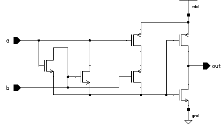 Figure 8.19: Circuit schematic of the Wang XOR gate.
Since the preprocessing stage drives more stages, all transistors in this stage are designed to allow faster operation. These cells are placed on top of a row of FA cells. It is very important that the pitch of these cells matches the pitch of FA cells. Otherwise, each block would need to be connected separately and the resulting routing would have significant area overhead.
The basic graph of the 10-bit parallel prefix adder in Figure 8.18 shows that four rows of delta functions would be necessary to realize the carry propagate function. It was also considered to use only three rows (as two rows only needed 2 Delta cells while the remaining two rows used 4 cells). The problem lies in that the output of these cells have to be fed into the next stage. When the Delta cells are not placed in their rows this would mean re routing the signal backwards. It was found that this solution would work for certain cases (it was used in the accumulator which uses four rows instead of the required five ) but would complicate the routing and generality of the circuit too much. As at most 4 blocks per row are used, these blocks are designed to be two times as wide as the preprocessing blocks and their height was minimized.
This cell again must match the width of the FA cells. It consists of the same XOR that is used for the preprocessing stage (with smaller transistor dimensions) and a pipeline register which is the same DFF that is used throughout the design with slight modifications to have the required width.
Figure 8.20 shows the layouts of the three basic cells that are used in the Parallel Prefix Adder.
 Figure 8.20: Layouts of preprocessing cell(left), Delta cell(middle), postprocessing
cell (right) of the Parallel Prefix Adder.
Figure 8.20: Layouts of preprocessing cell(left), Delta cell(middle), postprocessing
cell (right) of the Parallel Prefix Adder.
The problem with the negative numbers and the solution was discussed in Section 6.1.4. The necessary logic cells (AND gates) can easily be added to the circuit and do not require any special design effort. Figure 8.21 shows the 3 AND gates that have been placed in front of the first row of FA's.
 Figure 8.21: Blocks inserted for negative numbers.
The Metal-2 lines to the bottom of the picture are the data inputs while the Metal-2 lines covering the AND gates are used to connect the Clk, Read and Read' signals of the Sense amplifiers between the two RAM blocks cells as well as the VDD and GND connections.
The systolic adder has also been described simulated and synthesized by a top down approach using VHDL (VHSIC Hardware Description Language) . The code given below was written for this purpose:
There are different methods for describing a behavioural model. The most simple one would involve the shifting and addition of four 10-bit numbers. The resulting code includes registers for individual operations so this description is not very useful. A more hardware level approach would be to describe the connections of various components which would correspond to literally describing the schematic. The method chosen here uses variables to force the synthesiser to generate a layout that performs these operations one after another without using registers to store intermediate results.
The circuit was simulated, verified and synthesized. The basic core area occupied by the synthesized standart cells is 500um x 420um (210.000um^2) \)which is more than double the size of the full custom solution. This comparison may still not be very fair for a few reasons:
There are important advantages of the synthesis approach. Designing the adder using the synthesis approach takes about one tenth of the time used to design a Full Custom Block. Furthermore, process migration is much simpler in the synthesis approach, changing a simple option within the synthesis environment is enough to map the design to a new technology (provided that standart cells exist for that technology). These two arguments are commonly used to describe the superiority of the synthesis approach.
For random logic structures, the synthesis- approach is simply unbeatable. For regular structures such as datapaths, systolic arrays and storage elements the verdict is not so clear. While the algorithm is mapped much faster into a gate level netlist, the actual placement and routing of these standart cells is much more complicated in a synthesized design. A full custom block is always designed with the signal flow and overall floorplan in mind, and the cells are designed to fit into the floorplan. The syntesized gate netlist on the other hand, contains no information and optimization about the signal flow and shape of the block. A second EDA tool has to be used to make the placement and routing of the actual design. The designer does not have direct access to the design (as the gate level netlist would not mean very much to the designer) and has to rely on this high level tool to make the routing. For a high performance design, the placement and routing step can take much longer design effort than writing the hardware description. New design tools try to address this problem in which sophisticated expert systems try to determine a-near optimal floorplan, automatically breaking the design into sub-blocks and setting optimization parameters for the synthesis of these blocks.
Full Custom design (for the design of regular structures) is not as difficult as some sources suggest it to be. As an example, the whole Aries block consists of the following design elements (only cells that are introduced in the stage are listed) :
This makes a total of 13 different blocks. The most complicated block that is listed here is the FA which has 28 transistors, all of the remaining blocks are much smallerwith respect to transistor count (at least five of the blocks described above can be called elementary blocks). Furthermore, any designer that employs a full custom design technique has most likely designed a number of different variations for most of the basic cells, thus only a few blocks have to designed from scratch. Even the cells that need to be re-adjusted to fit a certain area or meet a speed constraint, benefit from the design experience from earlier (similar) designs.
Speed optimization is another issue. First of all, the full custom designer has complete control over the design, and can make any adjustment that he/she feels necessary and can therefore determine all the critical factors that affect the operation speed such as block placement, interconnection and device sizing, precisely. As for the majority of the circuits, only a few cells (the ones that are on the critical path) need to be optimized for speed, this is also not a very difficult task.
Overall, for the design of regular structures the full custom layout design technique is not as obsolete as many sources would suggest. It offers the highest performance both in terms of area and speed, and the design time for high performance designs is comparable to that of synthesized designs, which have typically much lower performance.
In this thesis, a programmable LSI macro-block for Digital Signal Processing applications is presented. The proposed Aries architecture occupies a silicium area of less than 1.5mm^2 and can be used to construct digital filters of any dimensions (both 1-D and 2-D). An additional final adder can be used to form a pipelined adder chain that can accumulate the results of different Aries blocks. Aries can operate on data rates of up to 50 MHz, enabling it to be employed even in the most demanding high-resolution image filtering applications.
C. Piguet, "Ultra Low-Power Digital Design," in CMOS \& BiCMOS IC Design'97 , Lausanne, 1997.
L. Dadda, "Some Schemes for Parallel Multipliers," Alta Frequenza , vol 34, pp. 349-356, May, 1965.
C.I. Göknar, Personal Correpondance.
N.H.E. Weste and K. Eshraghian, "Principles of CMOS VLSI
Design," Addison Wesley , 1993. J. M. Rabaey, "Digital Integrated Circuits, A Design
Perspective," Prentice-Hall , 1996. H. -J. Pfleiderer, "Systolic Arrays," in Advanced
Digital IC Design, Lausanne, 1997.
 KGF
KGF