Aries: An LSI Macro-Block for DSP Applications
![[PREV]](PIC/back.gif)
![[TOC]](PIC/toc.gif)
![[NEXT]](PIC/fwd.gif)
A systolic structure is made up of an array of identical basic processing elements with same type of (similar) connections. The name systolic adder is actually misleading for this particular adder used within Aries. The name comes from the earlier adder design used within the Taurus architecture, where the partial results of all eight bitplanes were shifted and added in a single structure consisting of eight adder rows of five adders each (See Figure 3.6). In the present Aries architecture, the systolic adder is required to shift-add four numbers in each cycle, as a result of time multiplexing. Yet we have retained the name of this block, since the essence of the operation has not changed. This section will give an architectural overview of the designed adder. A detailed analysis discussing the design methodology will be presented in Chapter 8.
The algorithm in Aries requires that four numbers corresponding to the partial sums of bitplanes be added in one cycle. This operation can be summarized as:
 (6.1)
(6.1)
The multiplication with a power of two represents a shift-left operation. Symbolically this can be expressed like in Figure 6.1.
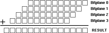 Figure 6.1: Symbolical representation of the shift-add operation used in Aries.
As no general building blocks for the addition of four binary numbers exist readily, this operation must be broken down into a simpler form so that it can be calculated with the basic CMOS building blocks. For the addition of more than two binary numbers (multi operarand addition), two different structures are commonly used [5]:
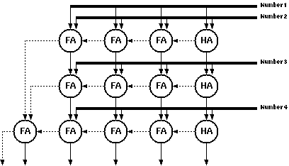 Figure 6.2: Multi-operand adder array with carry propagate adders.
Figure 6.2 shows the basic structure of a multi operand adder array which is constructed with carry propagate adders. This is called carry propagate because the carry from each adder is propagated directly to its neighbour. Only the sums of the adders within a row are passed to the next stage. The carries of all stages are evaluated with additional adders. The main disadvantage of this is the heavily serial nature of the operation. A worst case vector may cause the final result to be delayed more than m*n adder delays in an m x n adder array. A detailed analysis of the carry-ripple effect that causes this problem will be given in Section 6.1.2.
The carry output bit of a FA is by one order more significant than the sum output bit of the same adder. This is the reason why the carry is propagated in the carry propagate structure. It can be done differently though: In the carry save structure, the carry is saved, it is passed diagonally of the adder that is left to the adder that gets the sum output. This scheme is illustrated in Figure 6.3.
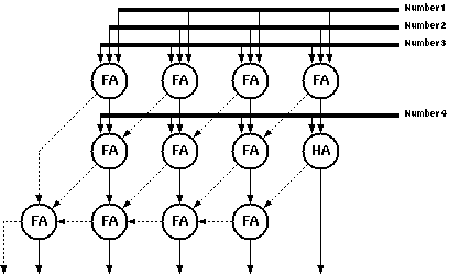 Figure 6.3: Multi-operand adder array with carry save adders.
Notice that the last stage in the figure is in fact another carry propagate adder. The carries are saved until the last operation, which leaves two vectors; one consisting of the sum and the other of the carries of the previous operations. Needless to say, these two numbers have to be added. If the simple carry propagate adder is used as the last step the worst case delay will be m+n for an adder array of the dimensions m*n. This can even be enhanced if a faster adder is used as the final adder.
![[TOP]](PIC/up.gif)
The most basic addition block that is used is the half adder. The half adder has only two 1-bit inputs, A and B, whose Sum can be calculated by a simple XOR operation. The Sum output is sufficient to express the sum of two 1-bit numbers for three out of four possible inputs. The sum of A=1 and B=1 can not be expressed by a single bit and a result with a higher significance than the Sum is required. This result is known as the Carry-out which states that an overflow has occurred.
The 1-bit FA is an enhanced half adder circuit having an additional Carry-in signal, which enables it to be cascaded with other adders and therefore is commonly used as a basic building block for generic adder arrays. The truth table of the FA is given in Table 6.1. (The truth table of the half adder corresponds to the first four entries in the truth table where Carry-in=0)
Table 6.1:Truth table of 1-bit FA.
Carry-In  A  B    Carry-Out  Sum
    0     0  0        0       0
    0     0  1        0       1
    0     1  0        0       1
    0     1  1        1       0
    1     0  0        0       1
    1     0  1        1       0
    1     1  0        1       0
    1     1  1        1       1
As the FA is the most widely used structure in a wide range of computationally complex functions, a significant amount of research effort was made on the realization of efficient adder structures. A quick glance to the truth table clearly reveals a classical XOR behaviour. XOR type functions typically have difficult CMOS realizations. A number of different realizations of FA's have been published [4,21,22,23,24] A well known CMOS FA structure was chosen in Aries since this adder is one of the most compact, robust and fast FA alternatives. The detailed design of a high performance FA cell, based on this adder, will be discussed in Section 8.3.2. The schematic of the adder and the transistor dimensions are shown in Figure 6.4.
 Figure 6.4: Circuit schematic of the CMOS FA.
Please note that in this implementation, Carry' is used to generate Sum; as a result the Carry signal can be generated before the Sum signal.
A total of n 1-bit FA's can be used to add two n-bit binary numbers (to be more precise n-1 FA's and a half adder, as the first addition would normally not have a Carry-in. This arrangement of FA's, where the Carry-out signal of the FA is connected to the Carry-in signal of the FA that adds the next significant bits, is known as the Ripple Carry Adder. The generic arrangement of the ripple carry adder is given in Figure 6.5.
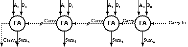 Figure 6.5: The Ripple Carry Adder.
Compared to all the known n-bit binary adders, the ripple carry adder is the most compact solution. It requires a small number of operational blocks (1 bit adders) and has a minimum routing overhead, as only the the Carry-out signals have to be connected to the Carry-in signals of the adjacent blocks. In a well designed layout of a FA circuit this connection can be made by simple abutment, which makes the design of the n-bit adder extremely simple.
The main drawback however, is that this realization is also the slowest parallel solution available. Although the adder accepts data in parallel, the operation is inherently serial because the addition of the i.th bit needs the Carry-out of the (i-1)th bit for the correct result. Starting from bit 0, the actual Carry is generated and rippled through all the stages to create the final result, hence the name ripple carry adder. The worst case scenario is when the carry of the first bit causes all the Sum bits to change. The delay for this operation is roughly expressed as n FA delays.
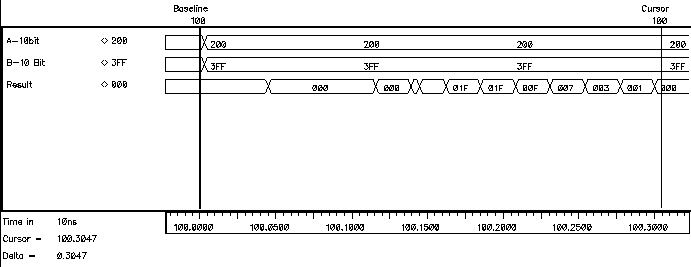 Figure 6.6: Simulated ripple effect in a 10-bit Ripple Carry Adder.
The behavioural simulation of a 10-bit Ripple Carry Adder in Figure 6.6 shows a worst case where A=(00 0000 0001) and B=(11 1111 1111) are added. All adders except for the adder of the least significant bits produce Carry-out=0 and Sum=1. Carry--out is available from the first adder (which in this case was at logic "0" prior to the addition) at the very first instant. As a result of the addition of the least significant bits (both of which are logic "1") a Carry-out=1 signal is generated by the first FA . With the arrival of this new (updated) signal the second FA starts calculating the correct result, generating another Carry-out=1 which in turn effects the third and all the subsequent stages. The carry generated by the first adder ripples through all the stages, causing subsequent transition of the sum bits. This is clearly visible in Figure 6.6.
Although it is true that for a worst case situation the carry will have to pass through a total of n adder stages, the associated delay is not exactly equal to n FA delays, as the Carry-out signal, for most efficient realizations of a FA, is calculated in advance of the Sum output which makes the overall delay shorter than expected. It is also easy to design a FA that is extremely fast for a single, given worst case situation (with far worse responses for other situations). Examples of this misleading approach are present even in the most known literature [21]. There are detailed analyses of the delay of the Ripple Carry Adder in the literature [25], but for first order estimation, the aforementioned worst case delay approximation of n FA delays is a solid measure.
One of the most serious drawbacks of ripple-carry adders is that: the delay scales linearly with the bit length, making adders operating on bit lengths larger than 16 rather in effective. A common philosophy in the microelectronic design is that in most cases silicon area can be traded off in order to get achieve higher speed. Addition proves to be no exception for this philosophy. A number of methods including, the carry skip adder, carry select adder, conditional sum adder, carry increment adder and the more general carry lookahead adder have been proposed. All of these methods are based on pre-determining the carry signal of a number of stages before the Sum of the previous stages is available.
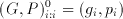
The parallel prefix adder [5] is a universal adder architecture that covers all of the known parallel adder structures described so far. The addition is described in three distinct steps:
Let A and B describe the two input signals that are associated with each stage. Two special signals are extracted from the inputs in preprocessing: propagate (p) and generate (g) signals. These two signals are said to describe how the Carry-out signal will be handled. A Carry-out could be generated within the block or the existing Carry-in signal could be propagated to Carry-out. These signals can be easily obtained from the available inputs as:
 (6.2)
(6.2)
 (6.3)
(6.3)
The i.th carry signal, Carry(i), can easily be expressed as:
 (6.4)
(6.4)
Likewise the i.th sum, Sum(i), can be calculated by:
 (6.5)
(6.5)
This is the task of the postprocessing step. This leaves only the Carry Propagation (Carry Lookahead) problem that needs to addressed. The carry propagation problem can be expressed in terms of a so called prefix problem where for a set of binary inputs (x(i):i=0,1,2,..,n) the outputs (y(i):0,1,2,..,n) are defined by the help of an associative binary operator Delta as:
 (3.3)
(3.3)
 (6.7)
(6.7)
The most important factor in this expression is that the Delta operator is associative:
 (6.8)
(6.8)
This sort of hierarchical organization brings in sub products which can be denoted as: Y^k(i:j), where k is the level within the hierarchy and i and j define the range that this sub product covers. For the carry propagation problem let us define the sub-product couple (G,P) such that:
(6.8)
 (6.9)
(6.9)
Where the desired
 (6.10)
regardless of the number of levels necessary to cover the range i:0. Given the two adjacent ranges a and b, the Delta operator performs the following logical operation:
 (6.11)
 (6.12)
 (6.13)
These equations reveal the following:
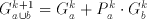
The graph representation of this problem provides a much clearer view of the algorithm. Two main symbols are used in the graph representation of prefix algorithms are given in Figure 6.7.
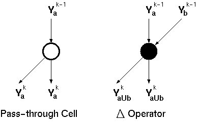 Figure 6.7: Two main blocks of prefix algorithm graph representations.
As a simple example, let us express the Ripple Carry Adder structure as a prefix problem. Figure 6.8 shows a prefix graph representation of a 16-bit Ripple Carry adder.
 Figure 6.8: Prefix graph representation of a 16-bit Ripple Carry Adder.
With the figure of the Ripple carry adder in mind we can easily define some performance measures for prefix adders:
The Sklansky parallel prefix algorithm is one of the fastest adder architectures, the graph representation is given in Figure 6.9.
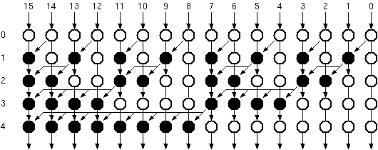 Figure 6.9: he graph representation of Sklansky Parallel Prefix Adder.
The main problems in the Sklansky Parallel Prefix Adder is that some nodes have pretty high fan-outs. Another alternative could be the Brent-Kung Parallel Prefix Adder which is shown in Figure 6.10.
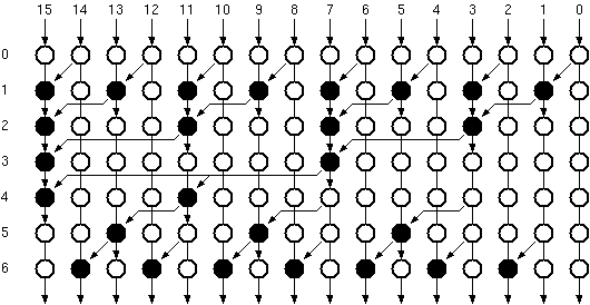 Figure 6.10: The graph representation of Brent-Kung Parallel Prefix Adder.
The Brent-Kung Parallel Prefix Adder is slower than the Sklansky Parallel Prefix Adder, but has less processing nodes as well as a much lower maximum fan out.
A generalized filter architecture must be able to cope with positive as well as negative coefficients. It is true that the hardware itself does not make distinctions according to the content of the data, thus performs the same operation regardless of the 'defined signs' of the operands. The problem however lies on the range boundaries of the number system used. The Two's Complement representation of negative numbers require a fixed data-length for proper operation. This accounts for extra complexity in shifted addition circuits where all operands have the same bit length but are shifted with respect to each other. The missing digits to the left of less significant operands have to be completed according to the sign of the operand. Luckily, this problem is easily solved as the last digit of any operand can be replicated to fill in the missing digits. A simple structure shown in Figure 6.11 controls this replication operation Aries, to enable a higher dynamic range for coefficients that consists of positive numbers only.
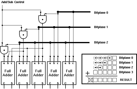 Figure 6.11: Adder Subtractor enhancement for the Systolic Adder.
The Carry Save Adder structure discussed earlier is the faster alternative for the Multiple Operand Adder used in the Systolic adder block. An operand bit length of 10 was found to be adequate for the design. As the capability to operate on negative numbers is also desired, the adder-subtractor enhancement discussed earlier was added to fill-in the missing digits. As a result of the negative number processing capability, the Carry-out of the whole block can safely be ignored which simplifies the design to some extend. The overall schematic of the Systolic adder is given in Figure 6.12.
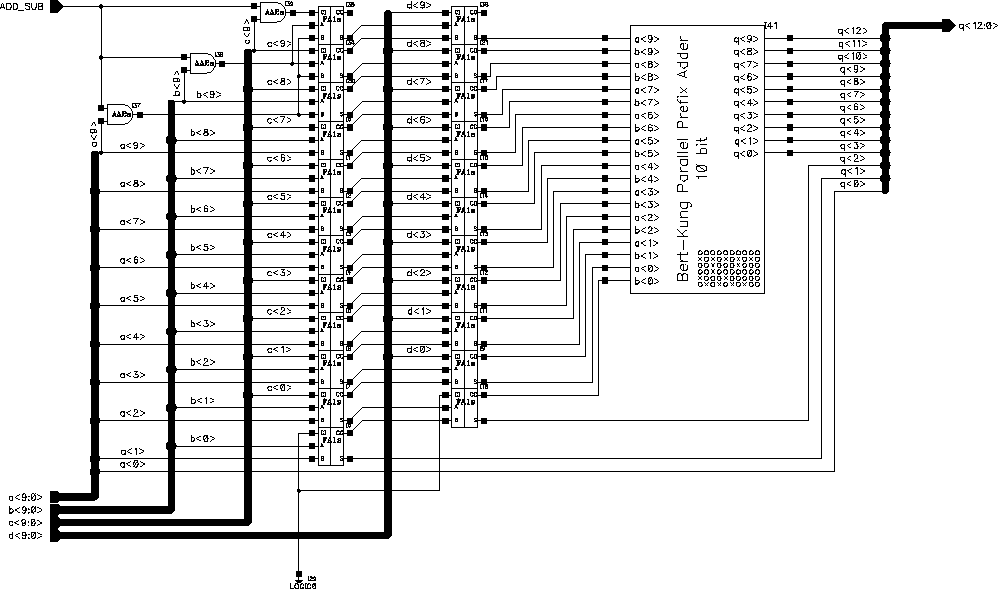 Figure 6.12: Schematic of the Systolic Adder.
The traditional Ripple Carry Adder scheme to calculate the final result from the two Carry and Sum vectors was replaced by a (modified) 10-bit Brent-Kung type Parallel Prefix Adder. It differs from a standart 10-bit adder in that the last Carry-out signal is not required and the carry propagate block is the same of that of a 9-bit adder. The general schematic of the modified Brent-Kung Parallel Prefix Adder is given in Figure 6.13.
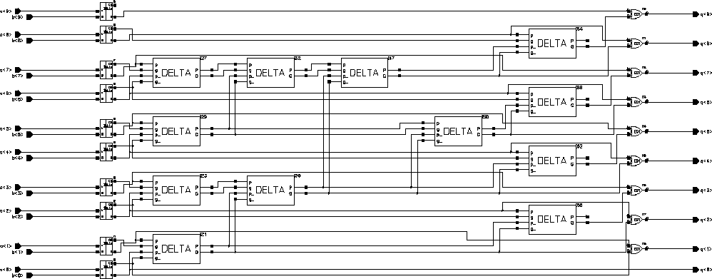 Figure 6.13: Schematic of the modified Brent-Kung Parallel Prefix Adder.
Please note that on both of the blocks the last Carry signals are left unconnected. The preprocessing blocks can be realized by simple half adders and the postprocessing block is a simple XOR gate. The "Delta" block actually performs the operation given in Equations 6.13 and 6.14, for which the schematic is given in Figure 6.14.
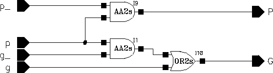 Figure 6.14: Schematic of the Delta block.
The final layout of the Systolic Adder including the pipeline registers is given in Figure 6.15. The adder dimensions, excluding the routing block at the bottom, are 320um x 300um in total.
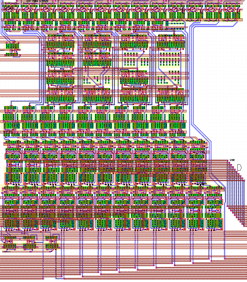 Figure 6.15: Final layout of the Systolic Adder.
Figure 6.16 shows a behavioural simulation showing the operation of the systolic adder. The four input vectors are named A, B, C and D respectively. The simulation starts with an initialization phase with all input vectors having a value of 0. At 10 ns four vectors are introduced to the systolic adder. All of these numbers are interpreted as positive numbers (operation mode is unsigned) and the result is calculated. At 20 ns, the vectors remain the same but the operation mode is changed from unsigned to two's complement. The first two vectors A=(11 1111 1000), B=(11 1111 1100), are interpreted as negative numbers and have corresponding weighted decimal values of A=-8 and B=-8. The result of this operation is 0. At 30 ns the first two vectors are changed to positive values. The result remains the same even after the mode of operation is changed to unsigned, since all vectors have the same value irrespective of the operation mode. The vector set which is applied at 50ns provides an interesting result. Although during both of the operation modes the result remains the same, the nature of operation in both cases is different. For the unsigned operation mode there is an overflow while for the two's complement operation the result is indeed 0. At 70ns a similar case with different vectors is tested, this time there is no overflow and the result is displayed correctly.
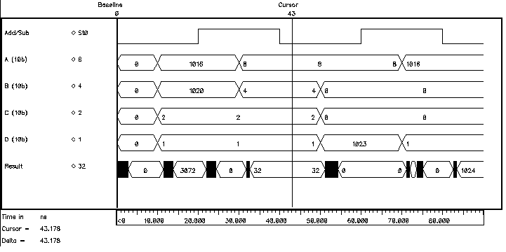 Figure 6.16: Behavioural simulation result of the systolic adder.
As described earlier in Section 4.1, Aries uses time domain multiplexing to simplify the hardware. While operating on 8-bit image data, the first 4-bit (nibble) is processed first and the result is stored in the accumulator. The same procedure is repeated for the second nibble. The accumulator adds this number to the stored result. As the second result is obtained from the higher-order nibble the result this time is actually 2^4=16 times the value it was calculated. Therefore, the second result has to be shifted by four digits to left prior to the final addition. The adder used in the accumulator is a 13-bit Brent-Kung Parallel Prefix Adder and was quickly designed by enhancing the Carry Propagation block for the additional bits. Once again a simple structure is used for negative coefficients compatibility. The schematic of the accumulator is given in Figure 6.17.
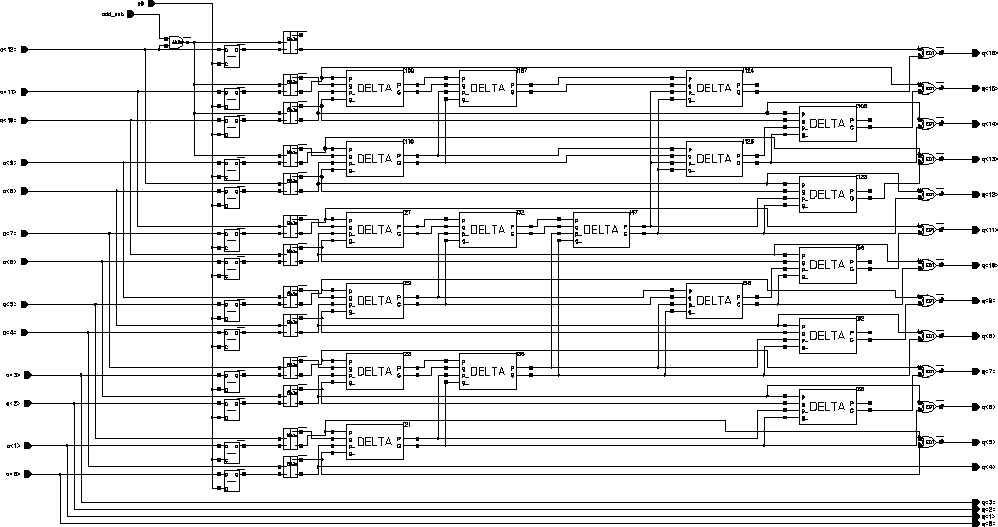 Figure 6.17: Schematic of the Accumulator.
The layout of the Accumulator block is shown in Figure 6.18, the layout dimensions are 340um x 200um in total.
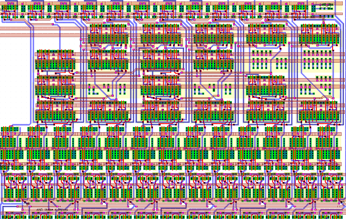 Figure 6.18: Layout of the Accumulator.
The registers within the accumulator block have different clocking signals. The systolic adder calculates a vector at every cycle, and the pipeline register samples this result at every cycle. The register within the accumulator block needs to sample the output of the pipeline register every two cycles when the result corresponding to the first four bits of data arrives. The result will be available at the end of next cycle. This result is sampled by the pipeline register following the accumulator stage. This timing is described in Figure 6.19
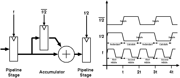 Figure 6.19: Block diagram and timing of the Accumulator.
This operation scheme has the disadvantage that some redundant calculations are made, specifically when the result from of the least significant 4-bitplanes are waiting to be sampled by the internal register they are shifted by four and summed up with the previously sampled sum of four least significant bitplanes. The result of this redundant operation is not sampled by the pipeline register. Needless to say this operation has no practical purpose and is totally redundant. To prevent the redundant calculations (and save power), a buffer stage could be used at the expense of silicon area, but as the redundant calculations do not produce any erroneous results this solution was not adopted for Aries.
To support negative numbers, the same solution that has been used in the systolic adder is employed. The last bit of the lower order operand is repeated to fill-in the missing bits. The only difference is that only one operand with four missing bits has to be filled instead of three operands with varying fill lengths. A simple AND gate is used to add a selective negative number processing capability.
The output of the accumulator is 17 bits long. In the earlier design phases it was decided that a barrel shifter be used to truncate this number to 8 bits. While this solution is ideal for a single block, it complicates the addition of partial results in the system level as outputs with different shifts have to be normalized before addition. Therefore, a unique high precision output is chosen. The least significant bit of the result is ignored in order to have a commonly used output of 16 bits. This truncation introduces some errors. Ignoring the least significant bit rounds positive numbers down while negative numbers are rounded up. This complicates the issue of correcting the error, since the error not only depends on the number system used but on the result as well. Table 6.2 summarizes all possibilities regarding the operands and the results and lists the corresponding error.
Table 6.2: Errors introduced by truncating the least significant bit.
Number System    1st Operand    2nd Operand    Result    Error

unsigned           positive       positive    positive    -.5
two's complement   positive       positive    positive    -.5
two's complement   positive       negative    positive    -.5
two's complement   positive       negative    negative    +.5
two's complement   negative       negative    negative    +.5
At first sight the error seems to depend solely on the result, but negative numbers are only a consequence of the different numbering system (two's complement). Any negative result in two's complement number representation format (a result with a MSB of logic "1") can be interpreted as a positive number in the unsigned number representation. The error caused by the truncation of the LSB will be different for both cases. Any rounding and/or truncation has an associated rounding error, but the error described above is an additional error to the conventional truncation error.
Since at any time all of the factors contributing to this error are exactly known (the result and the number system) it is possible to correct the truncation error. This correction can feasibly take place within the next stage, which is the Final Adder block. The overall Carry-In of the Final Adder can be used to compensate for the sign based rounding errors. Yet this approach was not used in Aries because the result of the accumulator can also be sent off-block by the output stage.
Figure 6.20 shows a simulation demonstrating the basic operation of the Accumulator. Both the input and the internal registers can be seen in the plot.
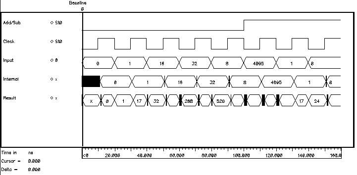 Figure 6.20: Simulation result of the Accumulator.
The output stage is not an internal block of Aries. It is intended to be used together with the final adder, to generate pipelined adder arrays to sum up the results of a number of Aries blocks. The details of combining several Aries blocks is discussed in detail in Section 7.3. The output stage determines the second operand of the Final Adder (the first operand of the Final Adder is always external), in which it decides:
The general block schematic of this stage is given in Figure 6.21.
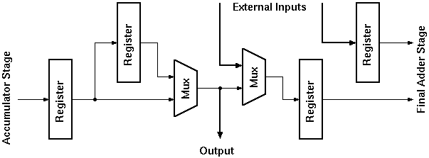 Figure 6.21: Block diagram of the output stage.
Two 2:1 multiplexers are used in the design. The first multiplexer controls the delay of the output while the last one selects either the internal data bus or an external data bus as the second operand for the final addition stage. Each of the multiplexers are controlled by a single bit giving four operational modes that are given in Table 6.3.
Table 6.3:Four different operating modes of the output stage.
   MUX-1          MUX-2                Operation Mode
Delay Select  Input Select   Accumulator Delay     Final Adder Operand
     0              0            No delay             Internal result
     0              1            No delay             External result
     1              0       1-pipeline stage delay    Internal result
     1              1       1-pipeline stage delay    External result
A very simple ripple carry adder structure is used as the final stage adder. The main purpose of this block is to allow cascading of Aries blocks to form a larger filter array. Since the output of the main Aries block is limited to 16 bits, a 16-bit adder structure is used within this block. Note that a simple ripple carry adder was used for the adder, as this block operates at half the speed of the internal adders. Initially the design of Aries consisted of a barrel shifter within the accumulator block which would provide 8-bit results. This solution was later given up to increase the resolution in the adder chains. Still, a simple ripple adder structure is sufficient to meet the speed requirements of the adder. The 16-bit sum of two operands has to be calculated in a pipeline stage within 20 ns which can easily accomplished by a ripple carry adder using the FA cell used throughout the design.
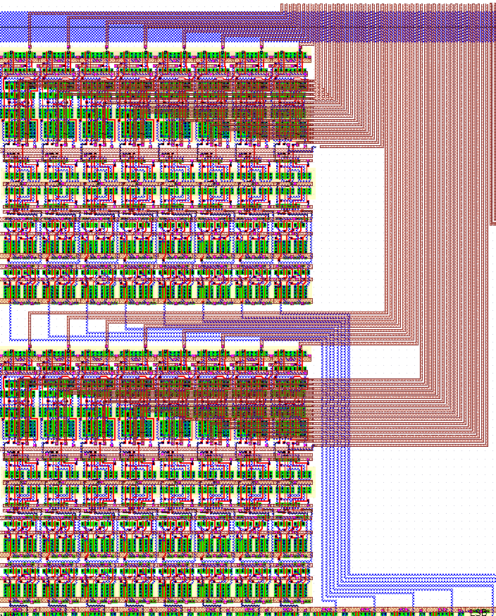 Figure 6.22: The layout of the output stage with the final adder.
The Figure 6.22 shows the layout of the output block with the final adder and all associated pipeline registers. The layout was designed and optimized for a 8-bit output stage in mind, and can not accommodate a 16-bit computation block. therefore the block is broken down to two 8-bit pieces. This scheme can be easily employed, as the ripple-carry adder used in the last stage can be broken down into two pieces without complicating the routing extensively (only the Carry-out signal of the last stage needs to be connected to the Carry-in of the subsequent stage).
 KGF
KGF