GALS System Design:
Side Channel Attack Secure Cryptographic Accelerators

Chapter 3:
Cryptographic Accelerators

Frank Kagan Gürkaynak
 
<kgf@ieee.org>

 
Disclaimer:
This is the www enabled version of my thesis. This has been converted from the sources of the original file by using TTH, some perl and some hand editing. There is also a PDF. This is essentially as it is, but includes formatting for A4, and some of the color pictures from the presentation.

Contents

1  Introduction
2  GALS System Design
3  Cryptographic Accelerators
    3.1  A Cryptology Primer
    3.2  Advanced Encryption Standard (AES)
    3.3  AES operations
        3.3.1  AddRoundKey
        3.3.2  SubBytes and InvSubBytes
        3.3.3  ShiftRows and InvShiftRows
        3.3.4  MixColumns and InvMixColumns
        3.3.5  Key Expansion
    3.4  AES Hardware Implementations
        3.4.1  Datapath Width
        3.4.2  Encryption/Decryption
        3.4.3  The AES Round Organization
        3.4.4  Roundkey Generation
        3.4.5  Comparison of AES chips
    3.5  Cryptographic Security
        3.5.1  Side Channel Attacks
        3.5.2  Differential Power Analysis
        3.5.3  Countermeasures Against Side Channel Attacks
        3.5.4  Implementation Issues
4  Secure AES Implementation Using GALS
5  Designing GALS Systems
6  Conclusion
A  'Guessing' Effort for Keys
B  List of Abbreviations
B  Bibliography
B  Footnotes

Chapter 3
Cryptographic Accelerators

3.1   A Cryptology Primer

The word 'cryptology' stems from the Latin word crypto that means 'hiding'. Surprisingly it is mostly associated with secret services, and dark sinister forces that forge evil plans to harm mankind. Throughout history, cryptology was mostly used to protect secrets. With the advent of the digital age, cryptology has transformed itself from a science that is used by the military and intelligence services to an essential part of the the digital information society.
Storing information digitally has many advantages. A digital content can (at least theoretically) be stored without loss or degradation indefinitely7. Not only that, but it can be copied, duplicated and transferred electronically with ease. Today, all sorts of information from simple letters to books, pictures, movies, medical records and business transactions are stored and transferred electronically in digital form.
Despite these advantages, there are some important problems associated with digital content. It can be changed at any time, without leaving a single trace. After all, it is not even possible to tell who has created a given digital information. Businesses that rely on distribution of information (news, music and media industry) do not take it too kindly that their revenue generating digital information can be copied freely either.
It is only with the help of cryptology that the above mentioned problems can be reliably addressed. The following is a list of some essential security services that are required in a working digital society.
Confidentiality:
The content of the information is kept secret. This is the basic service that is most commonly associated with cryptology.
Integrity:
The information has not been modified.
Authenticity:
The author (origin) of the information is known.
Access Control:
Access to information is restricted to certain users.
Non Repudiation:
The author of an information can not deny creating the information. This is important for digital transactions. Imagine a scenario where Alice places an order electronically. Once the order is completed, Alice should not be able to claim that she did not place the original order.
The branch of cryptology that is dedicated to develop methods that provide these services is called 'cryptography'. and systems providing these services are called cryptographic systems. The key part of a cryptographic system is a cryptographic algorithm that essentially provides a method to transform legible information (plaintext) into a form that is protected (ciphertext) with the help of a secret information (cipherkey).
The simple model given in figure 3.1 describes key components of a cryptographic algorithm. It has become common to personify the users of cryptographic systems 8. Alice and Bob are users of the crypto system and have access to a secret cipherkey. Oscar represents the malicious attacker who does not have access to the cipherkey, but is generally assumed to have unlimited access to the ciphertext. The process of transforming plaintext into ciphertext is known as encryption and the reverse process is known as decryption. The security of a cryptographic algorithm is defined by the difficulty in which the plaintext can be obtained from the ciphertext without knowing the cipherkey, a process known as 'breaking a cryptographic algorithm'. A second branch of cryptology, called cryptanalysis, concentrates on finding weaknesses of cryptographic algorithms and thus contributes to development of better (more resistant) algorithms.
Figure alice_bob
Figure 3.1: Simple model for cryptographic algorithms.
Designing cryptographic algorithms is a challenging process. The ultimate goal of such an algorithm is to achieve 'unconditional security'. An unconditionally secure algorithm can not be broken even with infinite amount of computation resources. Unfortunately, the practical realization of such algorithms have proven to be difficult9. What is more frequently used are 'computationally secure' algorithms. Breaking these algorithms requires a very large amount of computational resources. As long as the effort required to break the algorithm is sufficiently high10, the algorithm is considered to be secure. Most algorithms rely on well studied mathematical problems considered to be difficult to solve. There is, however, no proof that these problems can not be solved faster, because scientists were simply unable to do so over a long period of time. Cryptographers live in constant fear of a discovery that provides a faster solution to a mathematical problem serving as a foundation of their algorithm. This is the main reason that most modern cryptographic algorithms are required to go through a public review process.
Depending on how the cipherkey is managed, the cryptographic algorithms can be classified into publickey algorithms and privatekey algorithms. Publickey algorithms use a cipherkey that consists of two parts. Bob makes the public part of the cipherkey known to the whole world, and keeps the second part secret. When Alice wants to send a message to Bob, she uses this public key to encrypt the message. The public key algorithms are designed in a way to enable a decryption of the ciphertext only with the second (secret) part of the cipherkey. RSA [RSA78] is probably the best known publickey algorithm used today. Privatekey algorithms, on the other hand, rely on a cipherkey that both Alice and Bob know and keep secret.
Publickey algorithms are usually computationally intensive and are therefore not suited for secure transmission of lengthy messages. Privatekey algorithms are suited for bulk transmission, but it is a challenge to distribute the required secret cipherkey. Typical secure applications on the Internet use a public key algorithm to negotiate a sessionkey between Alice and Bob. This sessionkey is then used as the cipherkey of a privatekey algorithm to transfer data between Alice and Bob.
Privatekey cryptographic algorithms that use the same cipherkey to process multiple plaintext ciphertext pairs are called block ciphers. Common cryptographic algorithms like DES [Nat99] and its successor AES [Nat01a] fall into this category.

3.2   Advanced Encryption Standard (AES)

The first algorithm that was widely used in public is the Digital Encryption Standard (DES) algorithm that has been introduced as a U.S. federal standard in 1976. DES is a block cipher that operates on 64-bit words and uses a 56-bit cipherkey. DES (with its variations) was widely used for more than 20 years.
The main problem of the DES algorithm was its relatively short cipherkey, with 256 possible keys. Although this a fairly large number (72,057,594,037,927,936), with sufficient computational resources brute force attacks on DES are feasible. So-called DES challenges, where a large number of computers connected to the Internet exhaustively searched the key space, demonstrated this weakness dramatically. The first DES challenge in 1997 was completed in 4.5 months, the second in 1998 in 39 days and the third and final DES challenge in 1999 was completed in less than a day (22.5 hours) 11.
In 1997 the US National Institute of Standards and Technology (NIST) started a public competition to select an algorithm to replace DES. The algorithm was required to be a block cipher supporting cipherkey lengths of 128, 192, and 256 and to be free of any patents. The selection process consisted of several rounds where candidate algorithms were evaluated. At the end of the first round in August 1998, 15 algorithms were accepted as candidates. In the next round in August 1999, the candidates were reduced to five finalist algorithms (MARS, Blowfish, RC6, Rijndael, Serpent). Finally, in April 2000 the Rijndael algorithm was selected as the winner. On 2 October, 2000, NIST officially announced that Rijndael has been chosen as Advanced Encryption Standard (AES).
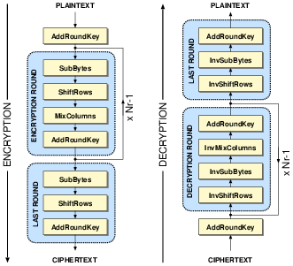
The AES algorithm is a block-cipher operating on 128-bit data blocks12 supporting three different cipherkey lengths of 128, 192 and 256 bits. These three flavors of the AES algorithm are also referred to as AES-128, AES-192 and AES-256, for 128, 192, and 256-bit cipherkeys, respectively. An AES encryption process consists of a number of encryption rounds (Nr) that depends on the length of the cipherkey. The standard calls for 10 rounds for AES-128, 12 rounds for a AES-192, and 14 rounds for a AES-256. During encryption, each round is composed of a set of four basic operations. The decryption process applies the inverse of these operations in reverse order. Figure 3.2 shows the basic structure of the AES encryption and decryption.
Figure aes
Figure 3.2: Basic structure of the AES algorithm: encryption (left), decryption (right).

3.3   AES operations

Figure state
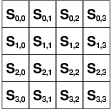
Figure 3.3: In AES, 128-bit data is represented as a four-by-four byte matrix called state.
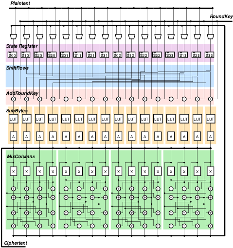
In the AES standard [Nat01a], the 'state' is defined as a byte matrix consisting of four rows and four columns as shown in figure 3.3. The element Sr,c is a 8-bit value that corresponds to the row r and column c of the state. A typical AES implementation uses a 128-bit state register as part of the round architecture. The operations that make up the AES algorithm are defined as operations that modify the state. The following subsections explain all operations in detail and provide a discussion on their implementations in hardware. All operations (except AddRoundKey, which is its own inverse) have a similar inverse operation. For clarity purposes, the text will refer to only the 'forward' operations in general descriptions. A block diagram of a complete AES encryption datapath is given in figure 3.4 for reference.
Figure aes_enc
Figure 3.4: Block diagram corresponding to a parallel 128-bit encryption only realization of AES as shown in figure 3.2. All operators and thin data connections are 8-bit and the thick lines represent 128-bit busses. (A) is the affine transformation and (X) is the xtime function.

3.3.1  AddRoundKey

During each round of an AES process, a separate 128-bit roundkey is used. The roundkeys are derived from the cipherkey using a key expansion routine. The AddRoundKey operation is a simple bit-by-bit XOR operation between the state and the roundkey. An AES process requires a total of Nr+1 AddRoundKey operations, as an additional 'initial' AddRoundKey operation is performed prior to the round operations. For an AES encryption process this initial AddRoundKey operation XORs the plaintext with the cipherkey. Since XOR is an involutory operation, AddRoundKey is used during the AES decryption process as well.
There is little that can be done in a hardware implementation to optimize the AddRoundKey operation, as it consists solely of XOR gates. Attempts to reduce the number of parallel XOR gates often require multiplexer structures that have an area overhead comparable to the area saved.
There is a need for an additional AddRoundKey operation during an AES process, as there are Nr rounds and Nr+1 subkeys. For most cases it is more efficient to implement a separate AddRoundKey function block in hardware for this additional operation than to share one block for all AddRoundKey operations.

3.3.2   SubBytes and InvSubBytes

Cryptographic algorithms require non-linear operations to be successful. SubBytes is the primary non-linear operation of the AES algorithm. It is an 8-bit transformation applied to each byte of the state independently. It consists of two separate transformations:
  1. The multiplicative inverse of each state byte in the finite field GF(28) is taken13. The hexadecimal value 0x00 is mapped on to itself.
  2. The affine transformation over GF(28) described by the following pseudo-code:

    -- Affine transformation in AES
    -- S(i) is the ith bit of the 8-bit input
    -- Z(i) is the ith bit of the 8-bit output
     
    Z(0) <= S(0) xor S(4) xor S(5) xor S(6) xor S(7) xor '0';
    Z(1) <= S(0) xor S(1) xor S(5) xor S(6) xor S(7) xor '1';
    Z(2) <= S(0) xor S(1) xor S(2) xor S(6) xor S(7) xor '1';
    Z(3) <= S(0) xor S(1) xor S(2) xor S(3) xor S(7) xor '0';
    Z(4) <= S(0) xor S(1) xor S(2) xor S(3) xor S(4) xor '0';
    Z(5) <= S(1) xor S(2) xor S(3) xor S(4) xor S(5) xor '0';
    Z(6) <= S(2) xor S(3) xor S(4) xor S(5) xor S(6) xor '1';
    Z(7) <= S(3) xor S(4) xor S(5) xor S(6) xor S(7) xor '1';

During a decryption process the InvSubBytes operation is used. It is similar in nature to the SubBytes operation and consists of the following two steps:
  1. The inverse affine transformation over GF(28) described by the following pseudo-code:

    -- Inverse Affine transformation in AES
    -- S(i) is the ith bit of the 8-bit input
    -- Z(i) is the ith bit of the 8-bit output
      
    Z(0) <= S(2) xor S(5) xor S(7) xor '0';
    Z(1) <= S(0) xor S(3) xor S(6) xor '1';
    Z(2) <= S(1) xor S(4) xor S(7) xor '1';
    Z(3) <= S(0) xor S(2) xor S(5) xor '0';
    Z(4) <= S(1) xor S(3) xor S(6) xor '0';
    Z(5) <= S(2) xor S(4) xor S(7) xor '0';
    Z(6) <= S(0) xor S(3) xor S(5) xor '1';
    Z(7) <= S(1) xor S(4) xor S(6) xor '1';

  2. The same multiplicative inverse for GF(28) that was used for SubBytes.
The performance of an AES chip depends mainly on the implementation of the SubBytes function. There are basically two main implementation choices for hardware: using a look-up table or applying arithmetic decomposition.
SubBytes is a 8-bit function. A look-up table that implements SubBytes contains 256 entries that are 8-bit wide. A mask ROM would be most suited for this purpose. However, ROM generators are technology dependent and are sometimes not directly available for a given technology. Full custom design is another alternative, but is a time-consuming process. A common, technology independent method is to map the look-up table to standard cells using a synthesis tool like the Synopsys design_analyzer.
Most modern FPGA architectures contain dedicated RAM arrays. AES implementations on FPGA's frequently make use of these RAM arrays by initializing them with the look-up table contents [MM03].
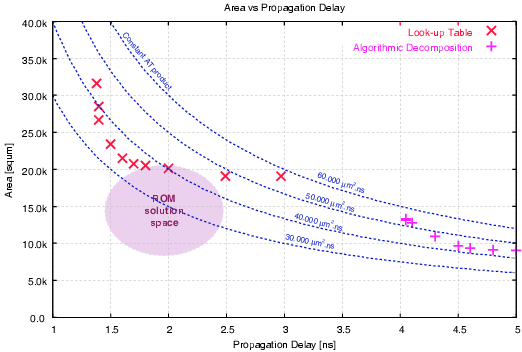
The second approach would be to find an algorithmic way to compute the SubBytes function. The main difficulty in this is the multiplicative inverse in GF(28) which requires excessive calculation and circuit area. However, an operation in GF(28) can be decomposed into operations in GF(24) as reported by Wolkerstorfer et al. [WOL02]. Figure 3.5 compares this approach to the synthesized look-up table. The multi-level architecture of the algorithmic decomposition results in a high propagation delay, compensated by the much smaller area. Overall, it can be clearly seen that both implementations share a common AT product. Figure 3.5 also contains the expected solution space for a mask ROM solution 14.
Figure sbox3
Figure 3.5: 8-bit SubBytes implementations in 0.25 m CMOS technology. A ROM generator does not exist for this particular technology. The figures for ROM have been obtained by full-custom design of SubBytes.
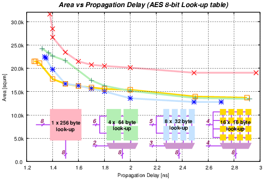
Traditional logic synthesis programs have difficulties in processing large look-up tables. Better results can be obtained by partitioning the look-up table into smaller ones. Figure 3.6 compares the circuit area and propagation delay of four different SubBytes implementations. Instead of using a single look-up table with 256 entries, the use of 8 look-up tables each with 32 entries can reduce the area by almost 30%. Experience has shown that the synthesized look-up tables result in netlists that require noticeably high routing overhead. It is difficult to quantify this overhead, as it is technology and library dependent, but it can result in noticeably larger circuits after the placement and routing phase.
Figure sbox2_4
Figure 3.6: Decomposing the look-up table for SubBytes can lead to more efficient implementations.

3.3.3  ShiftRows and InvShiftRows

The ShiftRows operation changes the order of bytes in each row of the state. The first row is not affected by this transformation. The second row is shifted cyclically to left by one byte, the third row by two and the fourth row by three bytes as seen in figure 3.7. The inverse operation InvShiftRows is quite similar in style, with only the cyclic shifts made to the right.
Figure ShiftRows
Figure 3.7: ShiftRows and InvShiftRows transformations. Shaded bytes are wrapped around as a result of the cyclic shift operations.
In a 128-bit parallel implementation of AES, ShiftRows can be implemented by wiring between operations without any hardware resources15. However, implementations that process fewer than 128-bits per clock cycle face a data-dependency problem. If no precautions are taken, the output of the first MixColumns operation following ShiftRows will replace unprocessed values in the state register. An obvious solution is to use an additional 128-bit round register. Depending on the round architecture, the amount of additional flip-flops can be reduced by clever scheduling of operations. However such elaborate organizations rely on selection circuitry, with additional area and propagation delay penalties.

3.3.4   MixColumns and InvMixColumns

MixColumns is a 32-bit operation that transforms four bytes of each column in the state. The new bytes of the column S¢r,c are obtained by the given constant matrix multiplication in GF(28). If the polynomial representation of binary numbers are used, this multiplication can be given as

é
ê
ê
ê
ê
ê
ë
S¢0,c
S¢1,c
S¢2,c
S¢3,c
ù
ú
ú
ú
ú
ú
û
=
é
ê
ê
ê
ê
ê
ë
x
x+1
1
1
1
x
x+1
1
1
1
x
x+1
x+1
1
1
x
ù
ú
ú
ú
ú
ú
û
· é
ê
ê
ê
ê
ê
ë
S0,c
S1,c
S2,c
S3,c
ù
ú
ú
ú
ú
ú
û
(3.1)
The addition in GF(28) is performed by the XOR operation. Multiplication on the other hand is more involved. A practical xtime function is defined for multiplication with x in GF(28). This xtime function can be described in the following pseudo-code:

-- xtime function
-- S(i) is the ith bit of the 8-bit input
-- Temp(i) is the ith bit of an 8-bit intermediate value
-- Z(i) is the ith bit of the 8-bit output
 
Temp(7 downto 0) <= S(6 downto 0) & '0';
 
if (S(7) = '1') then 
 Z <= Temp xor "00011011";
else
 Z <= Temp;
end if;

The Inverse function InvMixColumns is similar but requires a more complicated matrix multiplication:

é
ê
ê
ê
ê
ê
ë
S¢0,c
S¢1,c
S¢2,c
S¢3,c
ù
ú
ú
ú
ú
ú
û
=
é
ê
ê
ê
ê
ê
ë
x3+x2+x
x3+x+x
x3+x2+1
x3+1
x3+1
x3+x2+x
x3+x+x
x3+x2+1
x3+x2+1
x3+1
x3+x2+x
x3+x+x
x3+x+x
x3+x2+1
x3+1
x3+x2+x
ù
ú
ú
ú
ú
ú
û
· é
ê
ê
ê
ê
ê
ë
S0,c
S1,c
S2,c
S3,c
ù
ú
ú
ú
ú
ú
û
(3.2)
To obtain higher powers of x, the xtime function can be used repeatedly.
It is apparent from equations 3.1 and 3.2 that the InvMixColumns operation is more involved than that of MixColumns. Since all other operations in an AES round are more or less balanced in terms of both area and propagation delay, the difference in implementing MixColumns and InvMixColumns is directly reflected in the overall AES encryption and decryption performance. In a cryptographic system where a data stream is processed, the overall system speed is determined by the slowest of the encryption and decryption operations. In [GBG+04], this problem is examined in detail and a balanced architecture for both encryption and decryption is presented. This is obtained by optimizing the decryption path that includes the InvMixColumns operation aggressively to match the propagation delay of the encryption path. In terms of hardware complexity, the MixColumns operation can be mapped to a couple of stages of XOR gates and ends up requiring roughly 2-4 times more gate area than that required by the AddRoundKey function.
In the AES standard, the last encryption round does not require a MixColumns operation and similarly the last decryption does not require an InvMixColumns operation. Apparently this was made to allow a symmetric encryption and decryption flow. Hardware implementations hardly profit from this arrangement. Especially high-performance implementations suffer from additional hardware overhead to treat the last round differently.

3.3.5   Key Expansion

The key expansion routine is used to generate the roundkeys from the cipherkey. The AES standard defines the key expansion operations on four byte words called wi. A subkey is composed of four such words. The key expansion for AES-128 is relatively straightforward:
Unfortunately, the key expansion routine for other cipher key lengths introduces more irregularity to this basic process (see [Nat01a] for details). Implementations that support multiple cipher key lengths suffer excessively from this problem. Although the key expansion routine contains much less hardware than a regular AES round, the critical path of the AES system is more often located within the key expansion routine as a result of the flexibility required to implement different key lengths.

3.4   AES Hardware Implementations

Cryptographic algorithms are computationally demanding algorithms. Even powerful 64-bit micro-processors require hundreds of clock cycles to en/decrypt AES, which can be considered relatively software friendly. Public key algorithms like RSA may require as many as a million clock cycles on the same processor. The throughput of a cryptographic system is relevant when a continuous stream of data, such as video and audio streams are processed16. Such data streams may require processing rates from few Kbit/s to hundreds of Mbit/s. Especially for systems that require continuous execution of cryptographic operations, designing custom hardware to accelerate cryptographic operations is an efficient alternative to using general purpose micro-controllers.
Early stages of the AES evaluation process required "computationally efficient" implementations. Most algorithms developed for AES were primarily optimized for a Pentium system. Eventually, in the later stages of the evaluation, the candidate algorithms were also compared in terms of their suitability for hardware implementation. Several early papers [IKM00, WBRF00] provided a general overview without algorithm specific optimizations. In [LTG+02] two of the finalist algorithms (Serpent and Rijndael) were actually implemented in hardware.
After Rijndael was selected to be the AES standard, a relatively large number of AES hardware implementations were presented [VSK03, GBG+04, SMTM01, LT02, SLHW03, KMB03]. As described previously in section 3.3, AES consists of few simple hardware operations. The main factors determining the design of an AES hardware are described in more detail below.

3.4.1  Datapath Width

For a 128-bit parallel AES implementation as much as 80% of the area and more than 50% of the propagation delay is contributed by SubBytes, and the datapath width is practically determined by the number of parallel SubBytes operations performed in one clock cycle. Since 128 bits of data need to be processed during each AES round, the number of parallel SubBytes operation also directly determines the number of clock cycles required for an AES process. This represents a direct tradeoff between throughput and circuit area.
As described earlier, the ShiftRows operation can be realized without any special hardware resources for a 128-bit parallel implementation. However, AES datapaths that process less than 128 bits per clock cycle may be forced to either add additional intermediate registers or use extra clock cycles to overcome data dependency problems between ShiftRows and MixColumns.
In table 3.1, synthesis results from five AES encryption datapaths with different datapath widths are given for comparison. While smaller datapath widths result in a small architecture, they require additional selection circuitry between AES operators. This adds to the critical path, and increases the area.
Datapath Width8-bit16-bit32-bit64-bit128-bit
Parallel SubBytes units124816
Complexity (gate equivalents)5,0526,2817,15511,62820,410
Area (normalized)11.2661.4722.4324.269
Clock cycles for AES-12816080402010
Critical Path (normalized)1.3491.3411.2061.1331
Total time for AES-128 (normalized)21.58010.7294.8252.2271
Table 3.1: Synthesis results for five different datapath widths of a simplified AES encryption datapath. The additional hardware resources for ShiftRows have not been taken into account in this analysis.

3.4.2  Encryption/Decryption

One of the essential questions when designing custom AES hardware is whether or not the inverse AES process (AES decryption) is going to be supported. The NIST standard defines five operation modes for AES [Nat01b]:
Of these five modes, only ECB and CBC require the inverse AES operation for decryption. All other modes use a stream of AES encryptions to generate a pseudo-random sequence that are used to encrypt the plaintext. The decryption process for these modes requires exactly the same pseudo-random sequence that is generated by using the same stream of AES encryptions. Therefore, there are some systems where AES decryptions are not required at all.
Figure invsbox
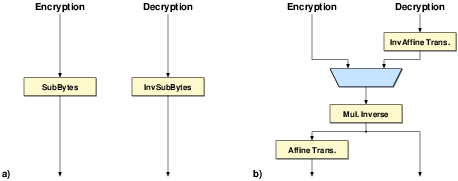
Figure 3.8: Two alternative realizations for implementing SubBytes and
InvSubBytes.
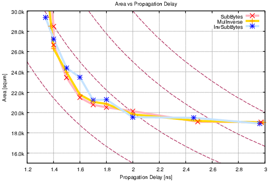
As the AES encryption and decryption processes are very similar to each other, a datapath that implements both functions is conceivable. The main problem in such an implementation is once again the SubBytes function. The inverse function InvSubBytes is equally complex and requires significant resources. Rather than using two separate functions as seen in figure 3.8a, both functions can be realized by sharing the multiplicative inverse. The resulting datapath will resemble the one shown in figure 3.8. When implemented as a synthesized look-up table all three functions (SubBytes, InvSubBytes, Multiplicative Inverse) require identical hardware resources (figure 3.9). The shared datapath as shown in figure 3.8b will result in a longer critical path due to additional transformations and selection circuitry. Designs targeting high throughput rates will often use a structure that supports only encryption or will employ separate datapaths for encryption and decryption.
Figure sbox1
Figure 3.9: Comparison of look-up tables implementing SubBytes, InvSubBytes and multiplicative inverse in GF(28). Synthesis results for 0.25 m CMOS technology.

3.4.3   The AES Round Organization

The goal of a hardware designer implementing AES is to come up with a datapath that implements the AES round efficiently. Such a round would generally contain one register for the state. Although the structure of the AES round has been defined in the standard for encryption and decryption, it is possible to re-order operations without changing the result.
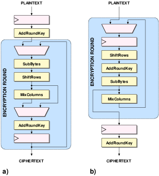
Figure 3.10 shows two possible organizations for the AES encryption round. A straightforward implementation of the algorithm (similar to figure 3.3) is given in figure 3.10a. The multiplexer between MixColumns and AddRoundKey is necessary for the last round of the encryption where the MixColumns operation is not executed. This multiplexer remains in the critical path throughout the entire operation. By re-ordering the operations, this multiplexer can be removed entirely from the hardware architecture. The ShiftRows operation is independent from both SubBytes and AddRoundKey and can be moved to a convenient location. The output is obtained by tapping into the hardware round after the SubBytes operation. In this organization, the additional AddRoundKey operation is executed separately at the end. This is not very costly, since AddRoundKey is the AES function with the least penalties for area and propagation delay. This architecture can be seen in figure 3.10b.
Figure reorder
Figure 3.10: Two different architectures for the AES encryption datapath: a) one to one implementation of the standard, b) re-ordered round structure with the additional AddRoundKey at the end.
A similar organization is made in [LTG+02] to insert a pipeline register into a datapath that supports both encryption and decryption. Separate organizations are used for encryption and decryption to find a suitable location to insert an additional pipeline register. Note that inserting pipeline registers may improve the clock rate of the system, but a higher throughput can only be obtained if independent data blocks are processed at the same time. Unfortunately, only ECB and CTR modes of operation can be used in such a pipelined system17.

3.4.4   Roundkey Generation

There are two main approaches to generate the roundkey used in the AES process. Keys can be generated on-the-fly by a concurrently executing datapath that computes the next roundkey during the time the actual datapath completes computing the current AES round. The second alternative is to pre-compute all roundkeys and store them in a roundkey memory.
A critical point in the implementation of a cryptographic system is the "key setup time" which is defined as the amount of time required to start cryptographic operations after a new cipherkey has been provided. On-the-fly key generators can be designed in a way to completely eliminate any latency overhead when changing cipherkeys, at least for encryption. For decryption, the first roundkey that is required is the last roundkey that has been used for encryption. Since the key expansion uses recursion, there is no simple way to obtain the last roundkey directly from the cipherkey. This must be done by computing all roundkeys for the encryption. The last roundkey so obtained can be used as an initial vector for the inverse key schedule.
The AES-256 mode requires 15 roundkeys with 128 bits. An on-the-fly key generator of a flexible AES implementation that supports both encryption and decryption for all standard key lengths needs to be able to store 256 bits of cipherkey, 128 bits for the roundkey, and finally 128 bits for the last roundkey. This is more than one fourth of the total amount of storage that is needed for all roundkeys. Consequently, pre-computing all roundkeys is not always a bad decision.
At first sight, the key expansion defined for AES (section 3.3.5) does not look hardware intensive. After all, only four SubBytes operations are required per AES round. However, the additional flexibility required to support all three key lengths results in a very cumbersome and slow implementation. For faster implementations with large parallel datapaths, the critical path through the key generator is usually longer than the actual datapath. For small implementations that use a datapath of 32 bits or less, more area is required to implement a key generator than the actual datapath.

3.4.5  Comparison of AES chips

There are many reported hardware implementations of AES in literature. Table offers a comparison of the key properties of these implementations. Ichikawa et al. [IKM00] presented a comparison of all AES candidates in hardware during the AES evaluation process. This early evaluation is not very representative, as no optimizations of any sort were made. The very large reported area is a result of a completely unrolled architecture for 10 hardware rounds. The reported throughput figure is a result of pipelining and only achievable in the ECB mode.
The implementations reported in [VSK03] and [KMB03] are high-speed designs that support three plaintext block sizes of 128, 192 and 256 bits as described in the original Rijndael specification. The additional block sizes, which are not part of the AES standard, add to the complexity. Both designs are capable of delivering higher throughput for these modes.
The SubBytes function has been implemented by using masked ROMs in [KMB03]. The high throughput reported by [SLHW03] is achieved by pipelining, which can not be used in feedback modes. This chip uses an algorithmic decomposition to implement the SubBytes function. Three of the four pipeline stages used in the round are dedicated to implementing the SubBytes function.
The design in [LT02] shares major datapath components between encryption and decryption. The SubBytes and its inverse is performed by using a single look-up table for the multiplicative inverse. A range of architectures with different datapath widths are presented in [SMTM01]. Unfortunately none of the architectures was implemented in silicon, and the presented results are from synthesis runs. While synthesis results certainly contain useful information and can be reliably used to compare different approaches, we have found it difficult to replicate the same performance obtained during synthesis after physical design. Most of the approaches and optimizations require large data buses with 128 bits or more to be distributed, and require significant amounts of selection circuitry, all of which are challenging tasks in the back-end design flow. Furthermore, look-up tables often employed in AES have very high demands on placement and routing. Some designs also use high clock rates and employ a large number of flip-flops, which results in severe clock distribution problems.
Verbauwhede
[VSK03]
Kim
[KMB03]
Satoh
[SMTM01]
Su
[SLHW03]
Lu
[LT02]
Ichikawa
[IKM00]
Technology0.18 m0.18 m0.11 m0.25 m0.25 m0.35 m
Area3.96 mm2N/A0.205 mm21.62 mm2N/AN/A
Gate Equivalents173,00028,62621,33763,40031,957612,834
RAM-4Kb-4Kb--
ROM-128Kb----
Throughput1600 Mb/s1640 Mb/s2600 Mb/s2970 Mb/s610 Mb/s1950 Mb/s
En/Decryptionencryptionboth/sharedbothbothboth/sharedboth
ModesallECBECB/CBCECBECBECB
Key Generationon-the-flystoredon-the-flystoredon-the-flystored
Key Lengths128/192/256128/192/256128128/192/256128128
Datapath256-bit256-bit128-bit128-bit128-bit128-bit
Notessupports 256-bit datasupports 256-bit datasynthesis results pipelinedsynthesis results unrolled rounds
synthesis results
Table 3.2: Comparison of AES implementations reported in literature.
A total of six different AES implementations in silicon have been designed at the IIS. A comparison of these architectures is listed in table . The first chip Riddler was designed by Adrian Lutz, Andres Erni and Stefan Reichmuth, as part of their semester thesis during the winter semester of 2001/2002. The goal of the semester thesis was to compare the two leading AES candidates Rijndael and Serpent with an emphasis on throughput. The students were in direct competition with a second group of students (Jürg Treichler, Gerard Basler and Pieter Rommens) that implemented the Serpent algorithm. The results were surprising [LTG+02]: both chips designed by teams with similar design experience within the same time, occupying exactly the same area (49 mm2 including pads in a 0.6 m CMOS technology) had almost the same measured throughput (around 2 Gb/s). Riddler uses two identical 128-bit AES rounds in parallel. The throughput figure is therefore only attainable for ECB and CTR modes of operation. The round structure uses a common multiplicative inverse look-up table, similar to the configuration shown in figure 3.8. The roundkeys are pre-computed and are stored in a register array.
Fastcore was designed by Franco Hug and Dominique Gasser during the 2002/2003 winter semester. The goal in this design was to support all operation modes and key lengths, and to obtain the highest possible throughput within a pre-determined core area (3.56 mm2 in a 0.25 m CMOS technology). The design has separate 128-bit encryption and decryption datapaths each with an independent on-the-fly key generator. As reported in [GBG+04] the design was optimized to have a balanced throughput for both decryption and encryption.
Riddler [LTG+02]Fastcore [GBG+04]Ares [PGH+04]BabyPampersAcacia
Technology0.6 m0.25 m0.25 m0.25 m0.25 m0.25 m
Area37.8 mm23.56 mm21.2 mm20.35 mm20.58 mm21.1 mm2
Gate Equivalents75,000119,00042,40814,25923,07639,012
RAM-----2Kb
ROM------
Throughput2160 Mb/s2120 Mb/s1150 Mb/s285 Mb/s230 Mb/s180 Mb/s
En/Decryptionboth/sharedconcurrentencryptionencryptionencryptionboth/shared
ModesECBallECB/OFBECB/OFBECB/OFBECB
Key Generationstoredon-the-flyon-the-flyon-the-flyon-the-flystored
Key Lengths128128/192/256128128/192/256128/192/256128/192/256
Datapath2 x 128-bit128-bit128-bit16-bit16-bit2 x 16-bit
Table 3.3: Comparison of AES implementations fabricated at the IIS.
During the summer of 2003, using a differential power analysis (DPA) attack, parts of the cipherkey were successfully recovered from a Fastcore chip [OGOP04]. This is the first reported successful DPA attack on an ASIC implementing the AES algorithm. The experience obtained from this attack has resulted in a string of AES designs that include countermeasures against DPA attacks. In his diploma thesis, Norbert Pramstaller investigated algorithmic countermeasures against DPA attacks[PGH+04]. The Ares chip was designed as part of this thesis during the winter semester of 2003/2004. The chip includes a 128-bit datapath and a separate (more flexible) 32-bit datapath both of which that support only 128-bit encryption. The numbers presented in table 3.3 are from the 128-bit core.
While all these chips were designed with primarily high throughput in mind, the Baby chip, by Peter Haldi and Stefan Zwicky during the 2004/2005 winter semester, was designed as a small and efficient AES implementation. This chip serves as a reference design for the Pampers chip that includes delay- and noise-based countermeasures against DPA. Pampers was developed by Stefan Achleitner as part of his diploma thesis during the 2004/2005 winter semester in parallel with Baby. Both designs use a dedicated key generator that supports all key lengths. Finally, Acacia, which will be explained in detail in chapter 4, is a GALS-based DPA-resistant AES implementation.

3.5  Cryptographic Security

As mentioned earlier in section 3.1, cryptographic systems are used to provide various security services. To illustrate the problems associated with these services let us consider the following smart card system used in private banking18. As part of a general strategy to increase customer satisfaction and reduce personnel costs, banks hand out so-called smart cards to account holders (users). By using Automated Teller Machines (ATM) that are located at convenient locations, the users are able to access a large portion of the bank services any time. Even in this relatively simple system different security aspects can be observed.
  1. Alice, who has an account at the bank, has an interest in protecting her bank account from others. The bank is primarily used as a safe place to deposit cash after all. Alice wants to be sure that only she is able to determine how money can be withdrawn from her account. Much like a regular house key, physical possession of the smart card is the primary method in which Alice is able to access her account.
  2. Oscar, who lives in the same fictional city as Alice, is a person with malicious intent. He is an expert in electronics, is extremely patient, and will consider all alternatives short of an armed robbery to get rich by manipulating bank services. He also knows all there is to know about the computing system of the bank.
  3. Alice is worried that, if she accidentally misplaces her smart card, Oscar could find it before her and instead of returning the smart card to her, he might decide to withdraw money from her bank account. The bank decides to implement a security system to comfort Alice. She is able to determine a password that is stored on the smart card. To access her bank account, Alice must use her smart card and correctly type in the password before using the ATM.
  4. Both the bank and Alice are worried about the fact that the communication from the ATM to the bank computer can be observed or even altered by Oscar. Therefore, the data transmission that contains the instructions from Alice to the bank, and information relayed back to Alice by the bank are encrypted. This sort of encryption needs a secret key that is known to both Alice and the bank.
  5. Since there are many similar account holders like Alice, the bank decides that it is more efficient to use the same secret key for all account holders. While the bank enjoys having Alice as a customer, it also does not want to entrust the secret to Alice directly. This is understandable, because Oscar might simply pose as an innocent customer, open a bank account at the same bank. By doing so he would receive a smart card himself and would automatically be given the same secret key. Oscar could then use his skill in wire tapping, to create mischief while Alice is using the system. As a solution, the bank decides to engrave the secret key into the smart card. Oscar can still obtain a smart card and try extracting the secret key, but the bank is convinced that Oscar will fail in all attempts in doing so.
  6. The ATM is another source of worry for both Alice and the Bank. Oscar has been known to place his own 'evil' ATMs that masquerade as the original 'good' ATMs. Alice does not trust any ATMs, as she does not know how to tell apart good and evil ATMs. The bank, afraid of losing good customers, adds another feature to its electronic banking system. Before the smart card exchanges any vital information with the ATM, it puts the ATM to a test. The smart card poses a question that can only be answered with explicit knowledge of the secret key. The evil machines prepared by Oscar would not know this secret. After all it is the desire to reveal this secret that drives Oscar to place these machines in the first place.
The first observation from this scenario is that a secure information system consists of several methods that are used in combination. The security of the overall system depends on the security of individual components. What is not discussed here, but is just as relevant, is the social side of the secure systems (see [And93] for some examples). For it is also possible to imagine Oscar trying to bribe, extort or somehow obtain the cooperation of bank employees.
When considering attacks on cryptographic systems, Oscar is assumed to have full knowledge of the entire system, but is considered not to posses any prior information on the secret key (Kerkhoffs Principle). The security of the system is defined by the effort that is required on part of Oscar to reveal the secret key. This directly defines the cost of breaking the system. A successful system is one where the benefits obtained by breaking the system is far less than the cost of performing such an attack.
The fact that Alice and Bob share a mutual secret (knowledge of the key), and their desire to exchange information, does not necessarily mean that they 'trust' each other. In the example above, the bank (imagine for arguments sake that the computer system of the bank is Bob) is not able to distinguish Alice from Oscar directly. Therefore the bank treats all its customers as a potential Oscar.
One of the main challenges in building a secure system is to find an adequate method of distributing the secret key used in various algorithms of the system. From a security point of view, it is desirable to use a different secret key for each user or even for each transaction of each user. This is however not always feasible. There are many instances, like the simplified smart card example above, where a secret key is embedded in a device that is available to all users of the system, including potential malicious users like Oscar.

3.5.1   Side Channel Attacks

Good cryptographic algorithms (like the AES algorithm presented in section 3.2) are designed to make it practically impossible to extract the cipher key by observing the outputs (known ciphertext attacks), or by providing specific inputs (chosen plaintext attacks). At least, the security in terms of the effort required by Oscar to perform a successful attack is well known and is deemed adequate for specific applications.
The implementation of a cryptographic algorithm results in a black box that has several observable physical properties such as power consumption, electromagnetic radiation, surface temperature, time required to complete an operation, or even sounds generated by this black box. All these properties that can be observed to change while cryptographic operations are processed, are information sources which can potentially be used by Oscar to reveal parts of the cipherkey. Such information sources are called side channels.
In 1996, Paul Kocher [Koc96] presented the first attack that used side channel information to determine parts of the cipherkey. In this attack "by carefully measuring the amount of time required for private key operations", the secret information used by several different cryptographic systems was revealed experimentally. This type of attack, where the secret information is revealed directly by measurement, is called simple side channel analysis attacks. Fortunately, these attacks are intuitive for both attackers and designers and are therefore (relatively) easy to defend against.
Soon after the first ideas were presented, cryptanalysts started to examine cryptographic hardware19 from different angles and were able to come up with different ways of exploiting side channels. It was soon discovered that side channel attacks which observe the power consumption are far more effective than other side channels. As a result, power analysis attacks became almost synonymous with side channel attacks20. For the remainder of this thesis only power analysis attacks will be considered as side channel attacks.

3.5.2   Differential Power Analysis

Little over three years after the discovery of side channel attacks, in 1999, Paul Kocher presented the first paper on Differential Power Analysis (DPA) [KJJ99]. In a DPA attack, the power consumption of a cryptographic device is measured while it processes a large set of cryptographic operations. In contrast to simple power analysis attacks, where the information is directly extracted from the measurements, DPA attacks use statistical methods to correlate the power measurement results to a set of hypothetical power consumption expectations. This method has been proven to be extremely efficient in attacking cryptographic hardware and has been a serious concern for developers of such hardware. In fact, in a joint work with S. Berna Örs from the Computer Security and Industrial Cryptography group of the KU-Leuven, we were able to successfully attack 8 bits of the cipherkey of the Fastcore AES chip, using a rather spartanic measurement setup, within only three days [OGOP04]21. After this point, our attention has focused on developing DPA resistant cryptographic hardware.
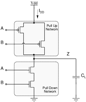
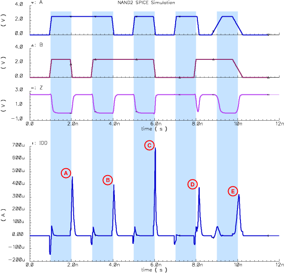
A DPA attack relies on the fact that the power consumption of a cryptographic hardware depends on the data that it processes. This is especially true for circuits using standard static CMOS logic style which is by far the most established method for implementing custom hardware at the moment. Figure 3.11 shows a simple 2-input NAND gate realized using standard static CMOS. The gate consists of a pull-up network that is activated to charge the output high, and a pull-down network that is used to charge the output low. The two networks are complementary, only one network is active at a time. Ideally, current only flows through the circuit when the output changes state, i.e. is charged from a low value ( GND) to a high value ( VDD) or vice versa.
The SPICE simulation in figure 3.11 shows the supply current of the NAND gate for different transitions of input. Even at this simplified simulation, it can be seen that the dynamic power consumption of the CMOS gate can differ significantly depending on a variety of factors. It can be clearly seen that only inputs that charge the output node from a low value to a high value result in a positive current to be drawn from the power supply.
In a typical AES implementation that is composed of tens of thousands of such gates, to determine the exact shape of the power supply current seems to be impossible. Thus, simple power analysis attacks at a gate level are highly infeasible. In the same way, it is also next to impossible to keep the power consumption of the cryptographic hardware identical when processing two different datawords. DPA takes advantage of this fact and is based on the variance of the power consumption.
Figure NAND2Figure measure3
Figure 3.11: Circuit diagram (left) and SPICE simulation result (right) of a 2 input NAND gate in static CMOS logic.
Overall, there are three factors contributing to the power consumption of a CMOS gate: static power due to leakage currents (Psta), short-circuit power due to non ideal switching characteristics (Psc), and the dynamic power consumed by charging or discharging the output load (Pdyn) [KL02]. If the contributions of Psta and Psc are neglected22, the total power P can be given with the well known equation (3.3).

P=Psta+Psc+Pdyn » a·f·CL·VDD2
(3.3)
If the supply voltage VDD and the operation frequency f can be considered constant for a given circuit, the only parameters that the designer can change are the load capacitance CL driven by the circuit, and the activity factor a. In effect, CL is determined by the netlist of the circuit and a is determined by the data that is being processed by the circuit.
Figure dpa
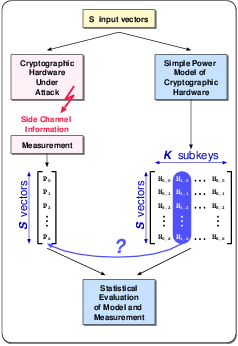
Figure 3.12: Simple representation of the DPA attack.
In a cryptographic algorithm, at some point the cipher key is combined with the data in some way. This leads to a power consumption that depends on the cipher key and on the data processed by the cryptographic device. DPA attacks target this specific operation of the algorithm. Rather than attacking the entire cipher key, only a part, called the subkey, is attacked at once23. The bit length of the subkey (m) is chosen so that a manageable number of subkey permutations exists. For an m bit subkey there will be K=2m subkey permutations. Figure 3.12 shows the principle of the DPA attack. Using a simple model of the circuit24, for each one of the K subkey permutations, S samples are processed and the hypothetical power consumption H1..K,1..S is calculated. Then the power consumption of the device is recorded while it processes the same S samples using the same unknown key. This leads to a vector P1..S, holding the different power consumptions for all S inputs. The correct subkey is revealed by correlating the hypothetical power consumptions H1..K,1..S with the measured power consumptions P1..S. In a successful attack, the correct subkey hypothesis Hkc,1..S will show a 'significantly' higher correlation to the measured power P1..S than all other subkey hypotheses.
Figure dpa_results
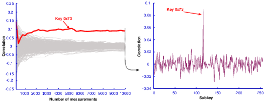
Figure 3.13: DPA attack results of the Fastcore chip [OGOP04]. The graph on the left shows the correlation of all K=256 subkey permutations to the measurement results as a function of the number of measured samples S. On the right, the correlation of all K=256 subkey permutations is given for S=10,000.
The results of a practical attack are shown in figure 3.13. The attack was performed on the Fastcore chip implementing the AES algorithm [OGOP04]. Fastcore was designed with purely performance in mind, and no countermeasures against DPA attacks were implemented. For this attack, a subkey of m=8 bits was targeted. The graph on the left of figure 3.13 shows the correlation of all K=256 subkey permutations to the actual measurements as a function of S. It can be seen that the attack requires few thousand measurements to be successful25. On the right hand side, the correlation of all subkey permutations is shown at S=10,000.

3.5.3   Countermeasures Against Side Channel Attacks

Developing countermeasures against DPA attacks has been an active research area ever since the discovery of the first attacks. The ultimate goal of DPA countermeasures is to increase the number of samples required to reveal the subkey to a level where it is not feasible to perform such attacks. In practice, DPA countermeasures are rated according to their relative effectiveness. A countermeasure that requires an attacker to perform 2S measurements to be successful will be considered twice as effective as a countermeasure that requires S measurements. As a hardware designer, it is important to understand the trade-offs between penalties involved (additional circuit area, loss in throughput) and the relative effectiveness offered by various DPA countermeasures.
DPA countermeasures fall into several categories:

Adding Noise

When measuring the power consumption in order to perform a DPA attack, actually only the part that is caused by an operation with the subkey is of interest. We refer to this part of the total power consumption as PQ. Part of the dynamic power measured during a DPA attack is totally independent from the data being processed, this portion of the power consumption will be called PR. Since the PR component will remain constant over all measurements, it will be filtered out during statistical analysis. There is a third component of the power that is consumed by gates whose inputs are uncorrelated to the attacked subkey and appear to be random. This component will be called PN. It is only this portion of the dynamic power that acts as 'noise' for DPA attacks. Mangard [Man04] evaluates the impact of the uncorrelated noise to the number of measurements. The higher PN, the higher the number of measurements S required to perform a successful attack. Assuming that the part of the circuit that generates PN uses the same supply voltage VDD and clock frequency f as the part generating PQ, equation (3) from [Man04] can be rewritten after substituting equation (3.3) as:

Var(Q)

Var(N)
» PQ

PN
= aQ·CL,Q

aN·CL,N
(3.4)
As can be seen from equation (3.4), the only way to increase the PN is to increase the switching activity aN or the load capacitance CL,N. Unfortunately the switching activity a can not be increased arbitrarily. A clock oscillator output would have a switching activity of 2, meaning that the output changes at twice every cycle. However, the load driven by this output would only generate a PR component. Theoretically, the maximum value for uncorrelated switching activity aN is 0.5. This is the case, when all of the nodes of the circuit change their value randomly.
Figure noise
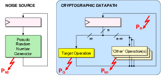
Figure 3.14: Adding a noise generator as a DPA countermeasure.
Let us consider the simple cryptographic datapath shown in figure 3.14. The datapath processes n bits of operation at a time. The particular DPA attack on this hardware targets only m bits. The information that is required for the DPA attack is contained in PQ. A large portion of the total consumed power of the cryptographic datapath can be contained in the PR part. As mentioned earlier, this portion has no consequence for this attack, no matter how large it may be in comparison to PQ. The remaining n-m bits of information will be processed by 'other' operators in the datapath. The power dissipation of these other operations will appear as PN1, as long as the n-m bits that are processed are not correlated to the m bits under attack.
In an attempt to increase the resistance against DPA attacks, a pseudo random number generating circuit can be added to the system in figure 3.14. Using equation (3.4), it can be derived that the uncorrelated dynamic power consumption contributed by the noise generator PN2 must be equal to

PN2
=
(b-1)·PN1
(3.5)
in order to increase the relative security of the original circuit by a factor of b. This can be re formulated as:

CL,N2=(b-1)· aN1

aN2
·CL,N1
(3.6)
A datapath optimized for implementing a cryptographic algorithm typically shows a high switching activity (aN1 in equation 3.6). This is a direct result of cryptographic algorithm specifications that typically require to switch half of its output bits, for a change of one bit at its inputs. Indeed, a post-layout analysis of an AES datapath shows a switching activity of slightly less than 0.3. A pseudo random number generator, such as an Linear Feedback Shift Register (LFSR), is used as a noise generator, since such circuits have an activity factor close to 0.526 (aN2 in equation 3.6). Therefore any effort to substantially increase PN2 has to find ways to increase the amount of switched capacitance CL,N2. In standard static CMOS circuits, the amount of switched capacitance consists of the input capacitances of the gates and the parasitic capacitances of the interconnects. Increasing either of them directly corresponds to increasing the circuit area. In principle, adding random number generators with large circuit area is the only way to attain high PN2. Adding noise is more efficient for cryptographic datapaths where not many uncorrelated bits are processed in parallel (low PN1). Cryptographic datapaths that process many parallel operations at the same time (high PN1) are less vulnerable to DPA attacks initially. To further increase their resistance against DPA attacks by adding noise generators is much more costly. On the plus side, the addition of noise generators does not interfere with the cryptographic operation and does not effect the throughput of the original circuit in any way.

Dummy Operations

When using DPA, the attacker needs to observe the power consumption of the same operation for a large number of samples. If the exact time when this particular operation is performed can be varied randomly, the attacker would be forced to collect more data. Clavier et al. [CCD00] describes DPA attacks on hardware protected by random process interrupts. This countermeasure, defined on a micro-controller system, basically interrupts the regular flow of the cryptographic process randomly with dummy instructions. The result is described as "smearing the peaks of differential trace due to desynchronization effect". The problem with this approach is that the dummy instructions might result in a observably different power consumption.
In a custom ASIC, this idea can be refined so that an external observer is not able to distinguish between a cryptographic operation from a Dummy Operation (DOP) that does not contain any activity related to the cryptographic procedure. If all datapath units within an ASIC are supplied with uncorrelated data during every cycle, it will not be possible to differentiate the operation through the power consumption. This holds true, even if no datapath unit performs an operation on data related to the cryptographic algorithm, i.e. when the ASIC performs a DOP.
When running a DPA attack, a certain cryptographic operation OPx is chosen where key dependent calculations are assumed to happen. Then, as described earlier, S measurements of the power consumption during clock cycle cy (that corresponds to the cycle during which OPx is executed) is sampled. If it is not possible to attribute the OPx to the clock cycle cy for each of the successive S measurements, the attack is hampered. If the probability of OPx being executed in clock cycle cy is defined as P(OPx,cy), the number of measurements required to perform an equivalent attack is given as [S/(P(OPx,cy))]. To protect a vulnerable operation OPx, a random number of DOPS (N) are executed at clock cycle cx prior to OPx. If N is evenly distributed, OPx will be executed somewhere in the interval cx..x+N, and the probability of P(OPx,cy), where y=x..x+N, will be [1/N].
As long as the DOP cycles can not be distinguished from cryptographic operation cycles, this countermeasure can significantly increase the number of measurements required for a successful attack with very limited or no apparent area penalty27. On the other hand, inserting DOPS directly increases the number of cycles required to complete the cryptographic procedure and therefore decreases the throughput of the system. Parallel implementations that have high throughput and require fewer cycles to complete the cryptographic procedure pay a higher price than small implementations, that require more clock cycles.

Alternative Logic Styles

DPA attacks can be completely inhibited, if the power consumption of the cryptographic device can be made totally independent of the processed data. Solving the DPA vulnerability entirely is a tempting prospect and as a result several approaches have been proposed. Asynchronous logic styles have been considered by Moore et al. [MAK00], or more recently a dual-rail pre charge logic style has been presented by K. Tiri and I. Verbauwhede [TV03]. A similar concept was also presented by Sokolov et al. [SMBY05].
The main challenge of facing designers of these new methodologies is that they are not 100% compatible with standard design methodologies. Some require the development of new standard cells, others require new design tools to complement existing methodologies, both of which are not extremely popular with the industry. It would be a major success if any one of these methodologies could present a solution that completely eliminates DPA attacks. Present results however suggest a significant reduction of emanated side channel information. While the relative security that can be obtained by adding noise sources or inserting dummy operations can be determined easily, the same can not be made for alternative logic styles. This makes it even harder to justify the application of a 'different' methodology.
While methods using alternative logic styles may effectively combat power analysis attacks, they may be vulnerable to other side channel attacks. Even though CMOS circuits were widely used and their properties were well known, it took years to discover that they could be attacked using power analysis attacks. Systems using such alternative logic styles will need to be put under the scrutiny of members of the cryptanalysis community so that their vulnerability against various side channel attacks can be fully explored. This is a Catch-22 problem, new logic styles are not put into use, as their side channel security has not been completely understood, and the cryptanalysis community concentrates its efforts mainly on systems that are widely available.

Algorithmic Methods: Masking

Figure masking
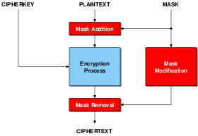
Figure 3.15: The masking method against DPA attacks. A random mask is added to the plaintext before each operation. This mask is removed at the end of the operation.
There are also solutions that try to solve the side channel problem on an algorithmic level [PGH+04, GT03,BGK04, AG02]. These countermeasures prevent direct operations between key and data by adding a random 'mask' to data prior to cryptographic operations as seen in figure 3.15. A DPA attack will require multiple runs, and for each of these runs a different mask will be used, effectively preventing the attack. At the end of the operation the mask needs to be removed. This is not very easy, as the mask at the output has been modified by the cryptographic algorithm as well. A dedicated mask modification block is used to predict the value of the mask that can be removed after the operation. In practice, this mask modification block is equivalent in size to that of the original circuit.
The principle of masking may seem very simple, but its implementation has many pitfalls. The mask addition is - by definition - redundant. An ideal logical optimization tool would be able to recognize this redundancy and would completely remove the masking part. Contemporary synthesis tools are far from achieving such an optimization. However, the practical realization of a masked algorithm requires many fine grained redundant operations that need to be processed in a specific way. The designer must invest significant effort in ensuring that the intended structure is present in the final netlist after logic synthesis.
On paper, masking countermeasures completely inhibit DPA attacks. However, Mangard et al. [MPG05] have recently shown that these masking methods are only effective if glitches do not occur in the circuit. It is ironic that practical realization problems hinder the effectiveness of an algorithmic countermeasure for a problem that arises as a result of practical implementation of an otherwise secure algorithm.

3.5.4  Implementation Issues

In practice, cryptographic ASICs need to be protected against a variety of threats, both electrical and physical. Various methods can be used to read out values of a circuit if physical access can be obtained. To protect against such attacks, tamper resistant design methodologies are used. In such a device the secret key is deleted as soon as a tampering attempt is detected.
All of the designs presented here are implemented as research chips and are not intended to be used in a cryptographic system. Unlike cryptographic products where the secret cipherkey can be embedded into the design by either an EEPROM or by mask programming, the chips presented here have interfaces that allow the secret cipherkey to be loaded and retrieved from the circuit. In addition, all have test interfaces that can be used to read out the state of all flip flops in the system, including those that hold the cipherkey.


File translated from TEX by TTH, version 3.77.
On 20 Dec 2006, 15:44.